|
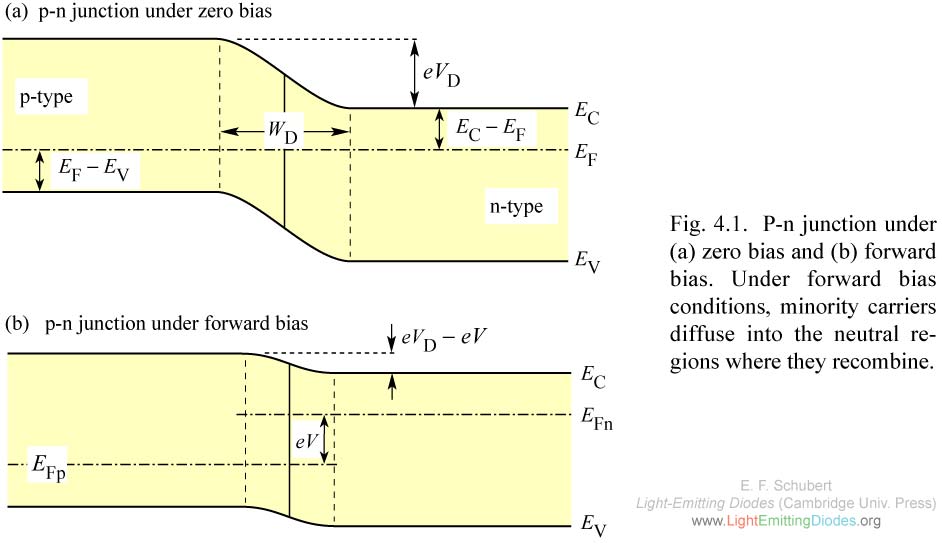
Fig. 4.1. P-n junction under (a) zero bias and (b) forward bias. Under forward bias conditions, minority carriers diffuse into the neutral re- gions where they recombine.
|
|
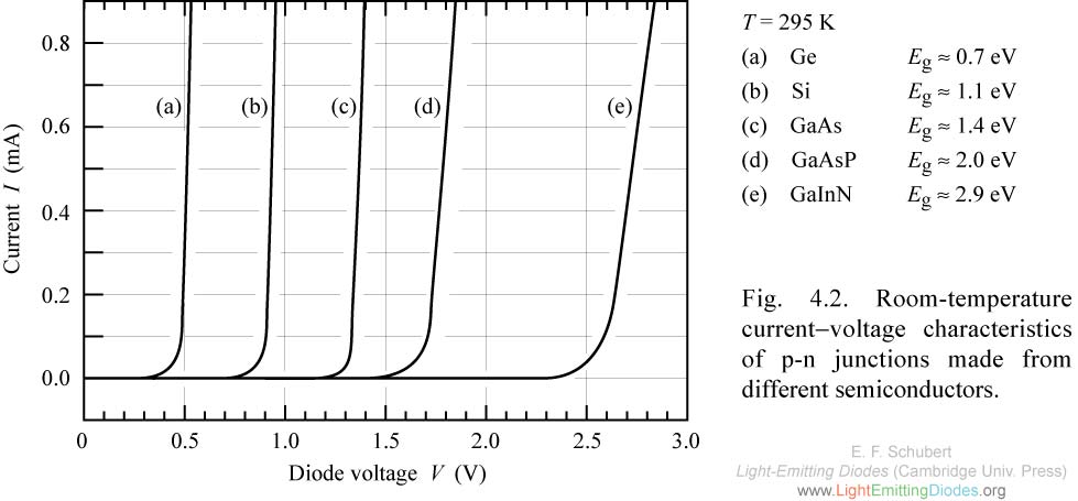
Fig. 4.2. Room-temperature current-voltage characteristics of p-n junctions made from different semiconductors.
|
|
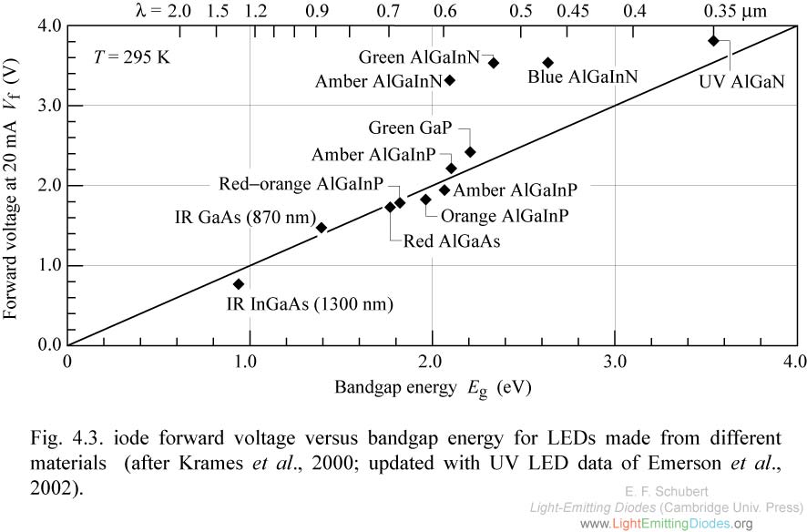
Fig. 4.3. iode forward voltage versus bandgap energy for LEDs made from different materials (after Krames et al., 2000; updated with UV LED data of Emerson et al., 2002).
|
|
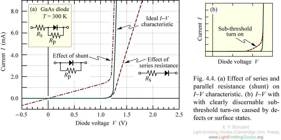
Fig. 4.4. (a) Effect of series and parallel resistance (shunt) on I-V characteristic. (b) I-V with with clearly discernable sub- threshold turn-on caused by de- fects or surface states.
|
|
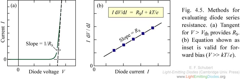
Fig. 4.5. Methods for evaluating diode series resistance. (a) Tangent for V > Vth provides Rs. (b) Equation shown as inset is valid for forward bias (V >> kT/e).
|
|
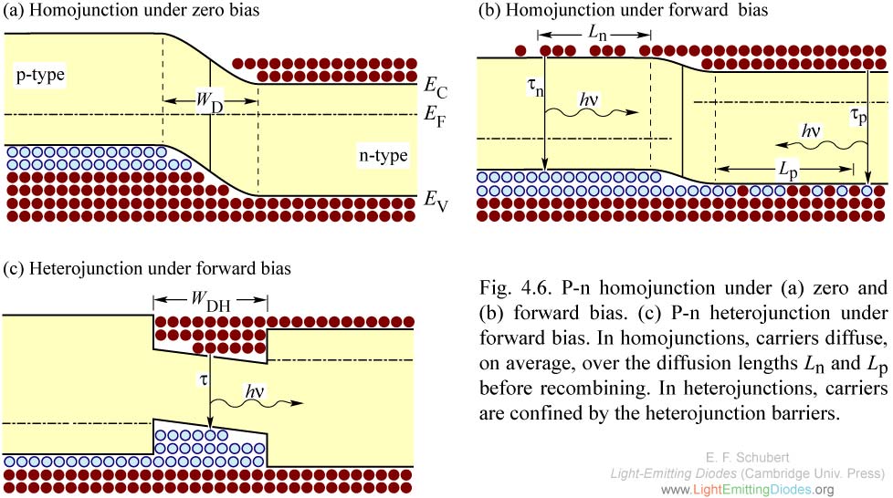
Fig. 4.6. P-n homojunction under (a) zero and (b) forward bias. (c) P-n heterojunction under forward bias. In homojunctions, carriers diffuse, on average, over the diffusion lengths Ln and Lp before recombining. In heterojunctions, carriers are confined by the heterojunction barriers.
|
|
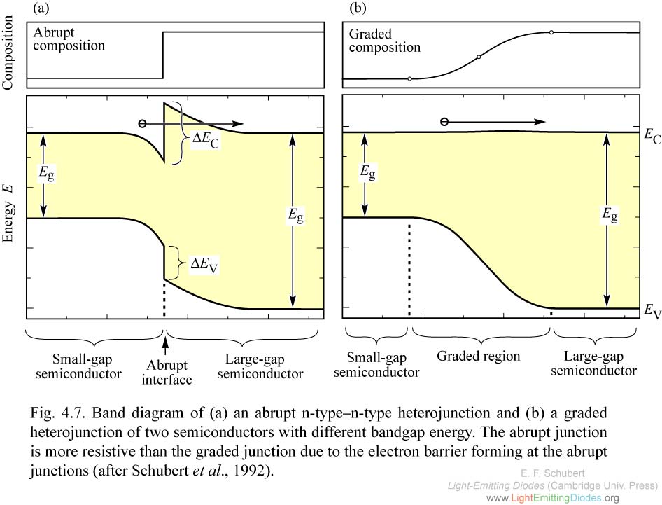
Fig. 4.7. Band diagram of (a) an abrupt n-type-n-type heterojunction and (b) a graded heterojunction of two semiconductors with different bandgap energy. The abrupt junction is more resistive than the graded junction due to the electron barrier forming at the abrupt junctions (after Schubert et al., 1992).
|
|
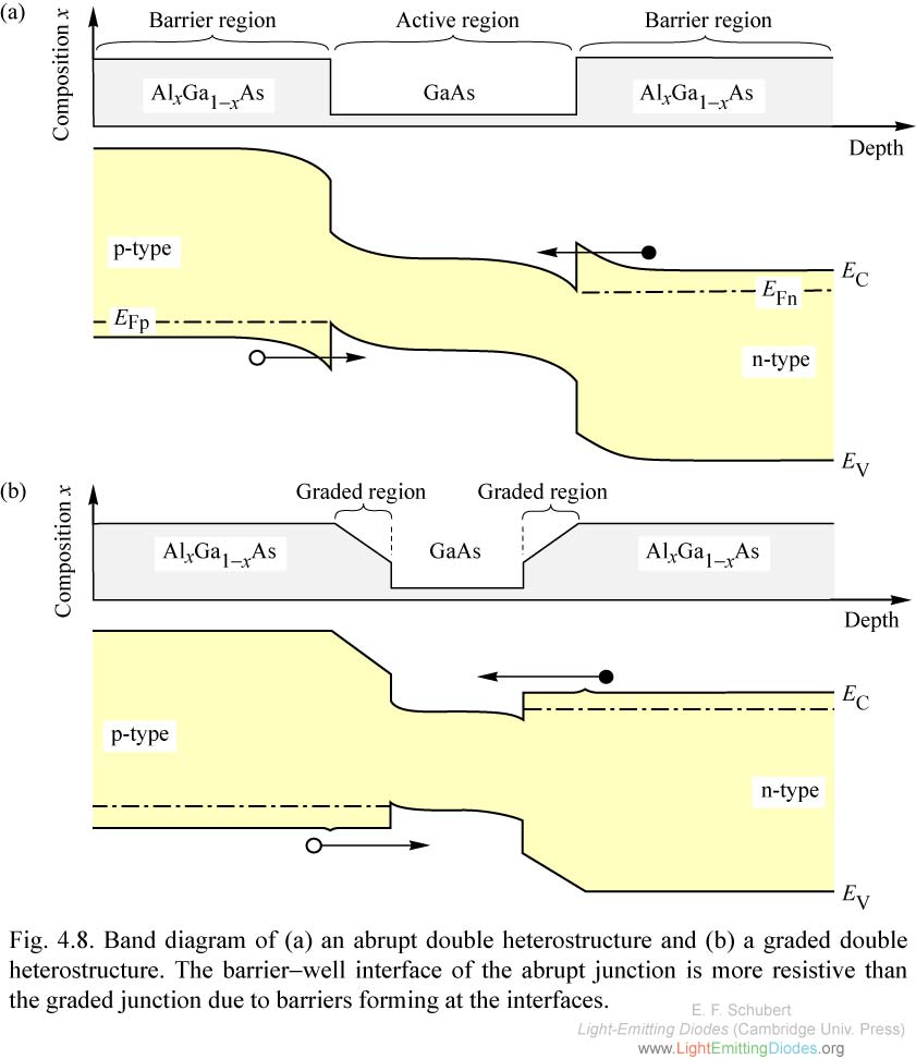
Fig. 4.8. Band diagram of (a) an abrupt double heterostructure and (b) a graded double heterostructure. The barrier-well interface of the abrupt junction is more resistive than the graded junction due to barriers forming at the interfaces.
|
|
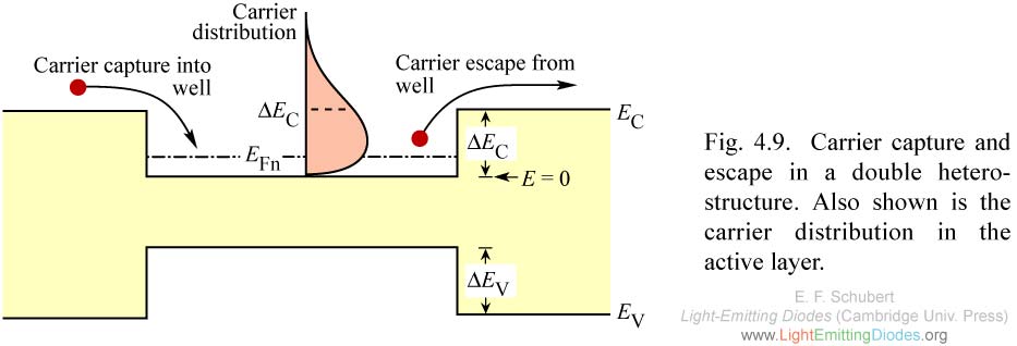
Fig. 4.9. Carrier capture and escape in a double hetero- structure. Also shown is the carrier distribution in the active layer.
|
|
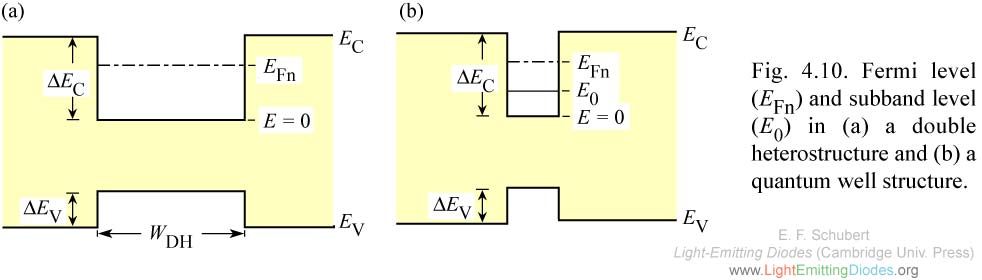
Fig. 4.10. Fermi level (EFn) and subband level (E0) in (a) a double heterostructure and (b) a quantum well structure.
|
|
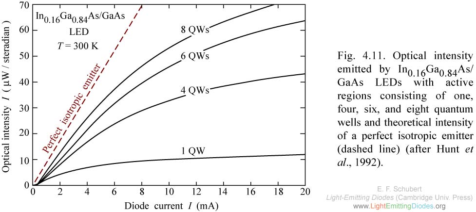
Fig. 4.11. Optical intensity emitted by In0.16Ga0.84As/ GaAs LEDs with active regions consisting of one, four, six, and eight quantum wells and theoretical intensity of a perfect isotropic emitter (dashed line) (after Hunt et al., 1992).
|
|
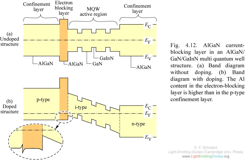
Fig. 4.12. AlGaN current- blocking layer in an AlGaN/ GaN/GaInN multi quantum well structure. (a) Band diagram without doping. (b) Band diagram with doping. The Al content in the electron-blocking layer is higher than in the p-type confinement layer.
|
|
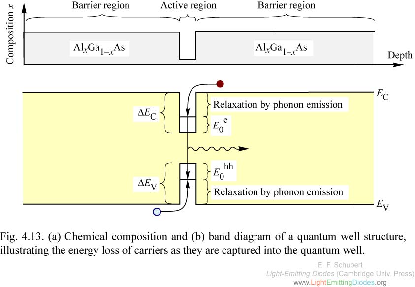
Fig. 4.13. (a) Chemical composition and (b) band diagram of a quantum well structure, illustrating the energy loss of carriers as they are captured into the quantum well.
|