|
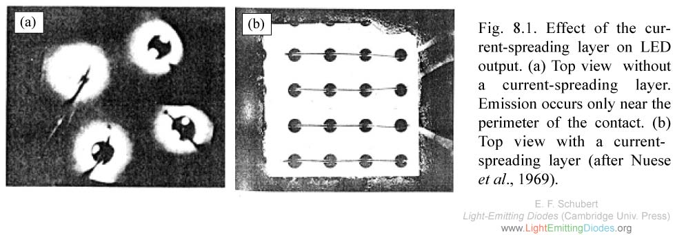
Fig. 8.1. Effect of the current-spreading layer on LED output. (a) Top view without a current-spreading layer. Emission occurs only near the perimeter of the contact. (b) Top view with a current-spreading layer (after Nuese et al., 1969).
|
|
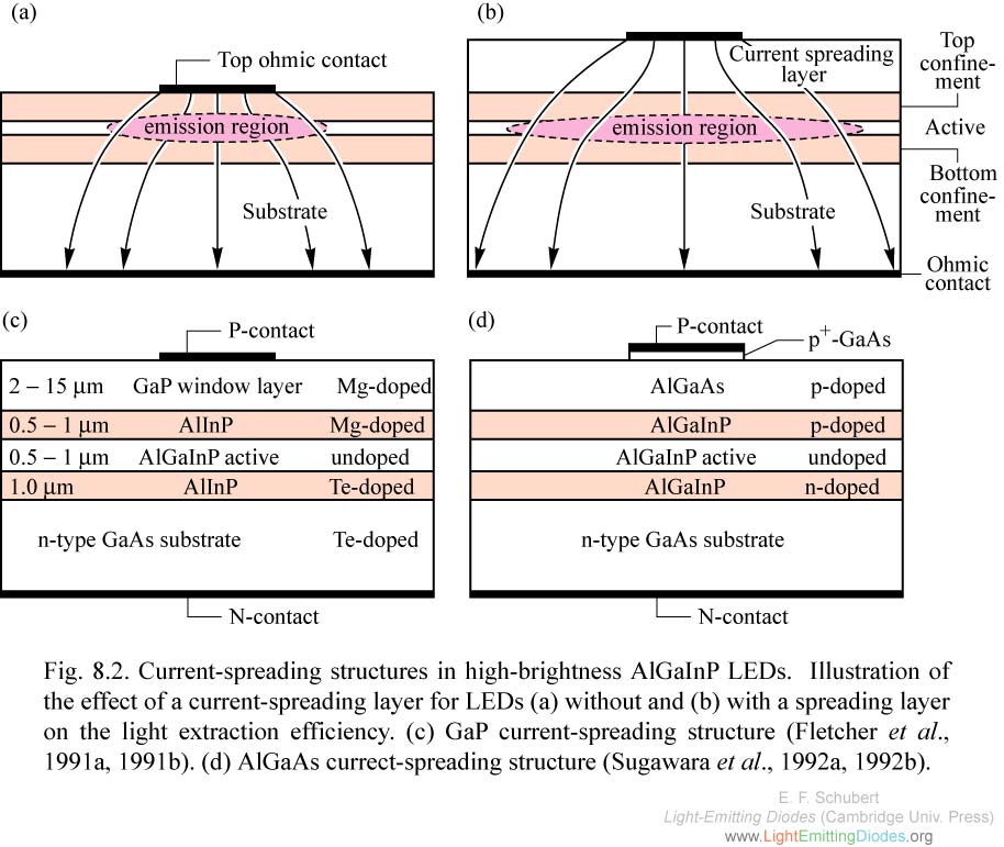
Fig. 8.2. Current-spreading structures in high-brightness AlGaInP LEDs.
|
|
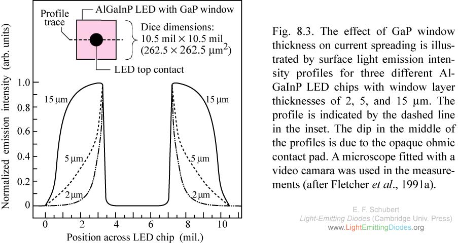
Fig. 8.3. The effect of GaP window thickness on current spreading is illustrated by surface light emission intensity profiles for three different AlGaInP LED chips with window layer thicknesses of 2, 5, and 15 mu m. The profile is indicated by the dashed line in the inset.
|
|
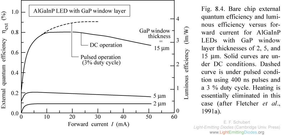
Fig. 8.4. Bare chip external quantum efficiency and luminous efficiency versus forward current for AlGaInP LEDs with GaP window layer thicknesses of 2, 5, and 15 micrometers.
|
|
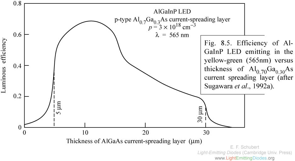
Fig. 8.5. Efficiency of AlGaInP LED emitting in the yellow-green (565nm) versus thickness of Al0.70Ga0.30As current spreading layer (after Sugawara et al., 1992a).
|
|
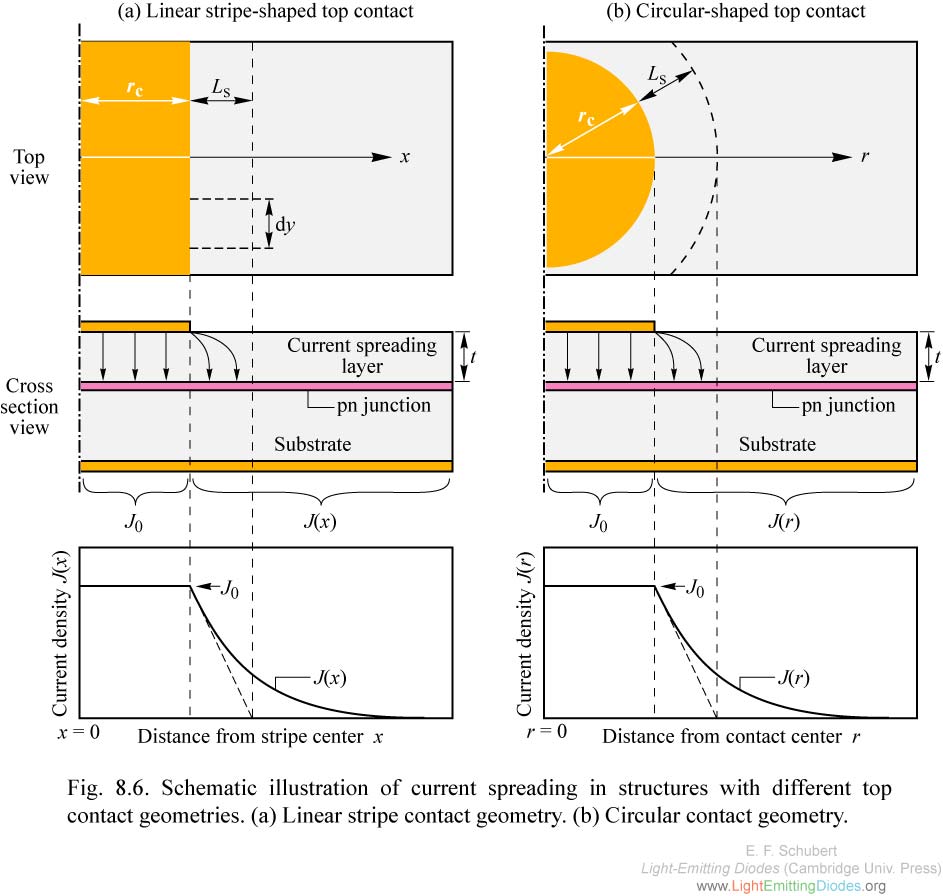
Fig. 8.6. Schematic illustration of current spreading in structures with different top contact geometries. (a) Linear stripe contact geometry. (b) Circular contact geometry.
|
|
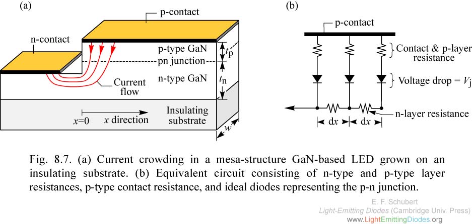
Fig. 8.7. (a) Current crowding in a mesa-structure GaN-based LED grown on an insulating substrate. (b) Equivalent circuit consisting of n-type and p-type layer resistances, p-type contact resistance, and ideal diodes representing the p-n junction.
|
|
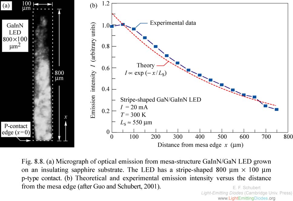
Fig. 8.8. (a) Micrograph of optical emission from mesa-structure GaInN/GaN LED grown on an insulating sapphire substrate. The LED has a stripe-shaped 800 mu m × 100 mu m p-type contact. (b) Theoretical and experimental emission intensity versus the distance from the mesa edge (after Guo and Schubert, 2001).
|
|
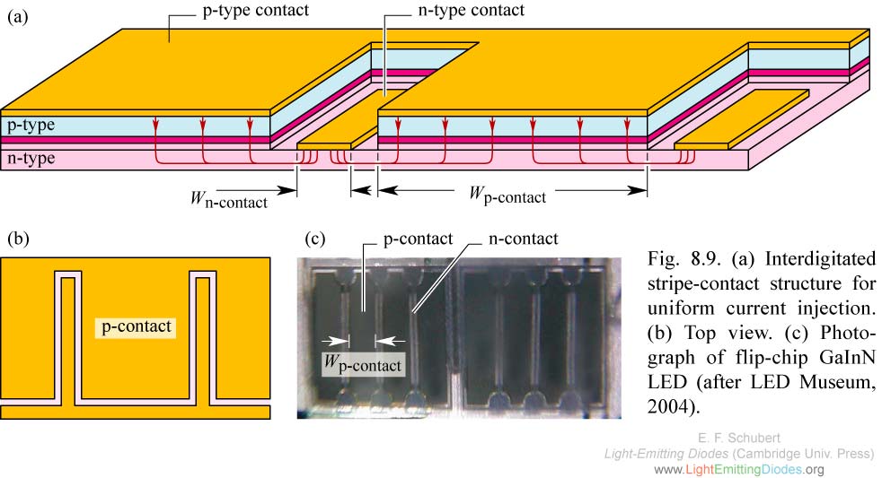
Fig. 8.9. (a) Interdigitated stripe-contact structure for uniform current injection. (b) Top view. (c) Photograph of flip-chip GaInN LED (after LED Museum, 2004).
|
|
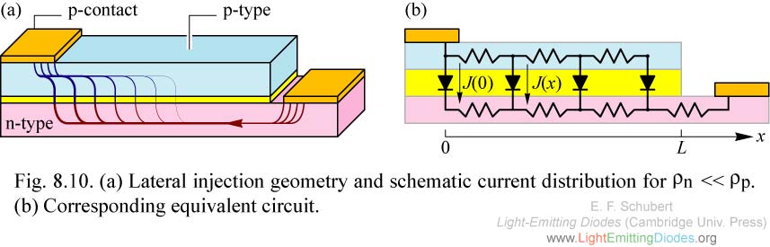
Fig. 8.10. (a) Lateral injection geometry and schematic current distribution for rho n << rho p. (b) Corresponding equivalent circuit.
|
|
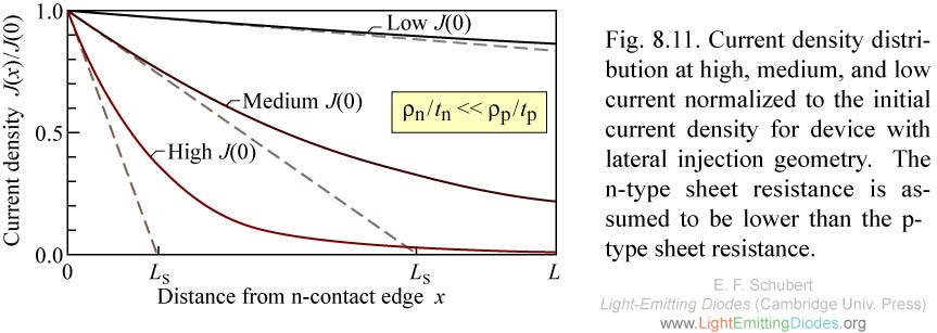
Fig. 8.11. Current density distribution at high, medium, and low current normalized to the initial current density for device with lateral injection geometry. The n-type sheet resistance is assumed to be lower than the p-type sheet resistance.
|
|
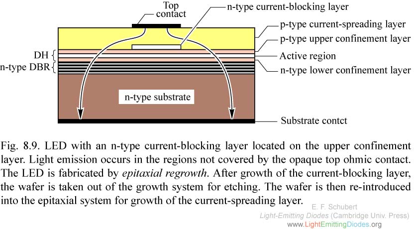
Fig. 8.12. LED with an n-type current-blocking layer located on the upper confinement layer. Light emission occurs in the regions not covered by the opaque top ohmic contact. The LED is fabricated by epitaxial regrowth.
|