
FIGURE 3.1: F-RISC / G SYSTEM
The F-RISC / G processor provided a test bed for many of the
ideas involved in implementing high speed cache memory hierarchies
in yield-limited technologies. Based on an evaluation of the F-RISC
/ G design space, a cache design was arrived at. A cache RAM and
a cache controller were designed and fabricated. The cache RAM
features a 0.75 ns read access time with dual data paths. The
RAM has 32 rows of 64 columns. The cache controller is configurable
for either instruction cache or data cache use. It contains a
Remote Program Counter (RPC) to eliminate address transfers in
the instruction cache except during BRANCHes.
The F-RISC architecture itself does little to constrain the design of the cache subsystem. In fact, except in extraordinary circumstances, the cache should be transparent to the CPU. As a result the architecture requires only that the cache store and retrieve data as required by the CPU. Write allocation policies, vertical memory communications, cache depths, and other design decisions matter only in so far as they affect the speed of the cache.
One architecture-imposed limitation, however, is the use of separate instruction and data caches, in which STOREs can take place only to the data cache (self-modifying code is therefore not permitted.)
While few of the design constraints on the F-RISC / G cache resulted
from architectural issues, the design of the F-RISC / G
core processor constrained the design of the cache to a great
degree.
FIGURE 3.1: F-RISC / G SYSTEM
A block diagram of the F-RISC/G system is given in Figure 3.1. The Central Processing Unit (CPU) is comprised of four datapath (DP) chips and a single instruction decoder (ID) chip. Instructions supplied by the instruction cache are decoded by the instruction decoder, which sends the decoded operands and control information to the datapath.
The data cache is used only for LOAD and STORE instructions (as with most RISC systems, F-RISC allows access to data memory only through these instructions.)
The Level 1 (L1) Cache is comprised of the primary instruction and data caches. Each cache consists of a single cache controller chip and eight RAM chips. Each of the two cache controllers must perform slightly different functions, but configuration circuitry is used to permit a single design to function in either the instruction or data cache. This was necessary in order to minimize fabrication costs, and minimizing the penalty of this decision represented a significant percentage of the design effort. The cache controller handles all handshaking with the secondary cache and the CPU, and sets the control lines of the RAMs as appropriate in order to direct the data flow between main memory and the CPU.
Each RAM chip is configured to store 32 rows of 64 bits and is single-ported. One unique feature of these chips, however, is that they have two distinct "personalities." Each RAM may read or write data four bits at a time using the DIN and DOUT buses. Each 64-bit row of memory may be filled one nibble at a time. A separate 64-bit bi-directional bus (L2BUS) allows reading or writing of an entire row at once. The wide bus is used to communicate directly with the secondary cache, and thus is less time critical than the four-bit bus which is used to communicate data directly to the CPU datapath.
Packaging delays play a major role in the critical paths for
the memory subsystem. Each cache must be able to handle one new
memory access each cycle. Were the processor and cache to operate
serially, this would require, for the data cache, that an address
be communicated from the datapath to the data cache controller,
that the tag be compared, that the address be forwarded to the
cache RAMs, that the RAMs perform a read and multiplex the appropriate
data to the output pads, and that the data be communicated back
to the datapath in less than a nanosecond. All of the memory subsystem
data critical paths are shown in Figure 3.2 while this particular
critical path is diagrammed in Figure 3.3.
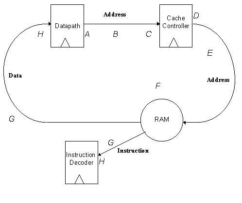
FIGURE 3.2: CRITICAL PATH
DIAGRAM
| Driver Delay + On-Chip Skew | |
| MCM Time of Flight + Skew | |
| Receiver Delay + 2 Multiplexor Delays + D-Latch Delay + On-Chip Skew | |
| Driver Delay + On-Chip Skew | |
| MCM Time of Flight + Skew | |
| RAM Read Access Time | |
| MCM Time of Flight + Skew | |
| Receiver + D-Latch Delay + On-Chip Skew |

FIGURE 3.3: DATA CACHE CRITICAL PATH
The access time of the cache RAMs was constrained largely by power consumption and heat dissipation issues; the faster the RAMs the more current is required to charge and discharge the bit lines, and the more heat that is generated and power that is consumed. The cache RAM blocks were designed to be accessed for reads in 450 ps, and the cache RAM as a whole requires 750 ps from address presentation to valid data output on the four-bit bus. This clearly makes it unlikely that the entire cache operation can be performed in 1 ns.
As a result the cache and CPU are pipelined, so the effective allowed time for the data cache is 2250 ps (1850 ps-2100 ps for the instruction cache). Specifically, two CPU pipeline stages are allocated for each memory operation. The instruction fetch takes place during the I1 and I2 stages of the CPU pipeline. Data reads take place during the D1 and D2 stages, while data writes are additionally allotted the DW stage. The D1 and I1 CPU stages correspond to the A cache stage, while the D2 and I2 stages correspond to the D cache stage [Phil93].
The data cache controller must be able to receive the address,
latch it, run it through a multiplexor (which is used to select
alternate address components in the event of a primary cache miss
- specifically the tag stored in the tag RAM), and drive it onto
the MCM lines. Allowing for slack and capacitive loading, 330
ps is a reasonable time allowance for these operations. A similar
amount of time should be allotted to the datapath to drive the
address and receive the data. This leaves approximately 840 ps
for communications between chips. Note that the address transfer
between the datapath and the cache controllers is further constrained
by latch clocking to approximately 500 ps (or, more precisely,
to approximately an integer number of clock phases - two phases
is the minimum attainable delay.)

FIGURE 3.4: SIGNAL TIME OF
FLIGHT
The time of flight, T, of electromagnetic signals through
an MCM with a substrate with dielectric constant r0
[Sze81] assuming lossless transmission lines is:
Figure 3.4 is a graph of signal time of flight on an MCM as a
function of dielectric constant. Assuming a dielectric constant
for Paralyne of 2.65 [Maji89] the time of flight on the MCM would
be 5.43 ps/mm. Allowing for clock skew between
chips, rise time degradation of MCM signals, and some slack due
to variations in MCM dielectric constant and dielectric thickness',
an MCM time of flight of 5.75 ps/mm is
reasonable for the purposes of this analysis. This would mean
that the total MCM distance allowed for this critical path is
approximately 146 mm. These times do not take into account the
resistance of the lines which results in an R-C charging effect
which increases rise time at both the drivers and the receivers;
it is hoped that these lines will be wide enough to minimize this
problem. If is the interconnect metal resistivity, l is
the line length, t is the interconnect thickness, and d
is the dielectric thickness, the R-C charging effect can be approximated
as [Salm93]:
Looking at this portion of the cache subsystem critical path more closely, the datapath chips and the cache controllers are each clocked by a global de-skewed system clock [Nah94]. The pipeline latch on the cache controller which receives the address from the CPU is clocked approximately 500 ps after the address is formed in the datapath. This means that there is 500 ps allowed for the datapath I/O drivers, the MCM time of flight, the cache I/O receivers, and associated skew, slack, and rise time degradation allowances.
Back-annotated simulations of the datapath chips show that the
address can be expected to be on the bus by 145 ps after phase
1. If 90 ps is allowed for on-chip and I/O receiver delays on
the cache controller, then the address must arrive at the cache
controllers by 410 ps after phase 1. This leaves 265 ps for the
actual communications to take place. The total path length for
these signals should therefore be less than 44 mm.
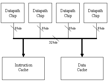
FIGURE 3.5: ADDRESS TRANSFER
FROM CPU TO CACHES
As shown in Figure 3.5, there are four datapath chips, each of which contribute eight bits to the address. The complete thirty-two bit address must be sent to both the data and instruction cache controllers. The total length of the the longest address line from any one of the datapath chips to both cache controllers should be less than 44 mm.
The next stage of the critical path is the transfer of the address
from the cache controller to the RAMs. Each cache controller must
send a 9-bit address to each of 8 RAMs. Were each cache controller
to incorporate only one set of address output drivers, then this
9-bit bus must be long enough to reach each of the eight RAM chips,
as shown in Figure 3.6. The total length of this bus would be
approximately 4 chip edges, or in excess of 40 mm, assuming all
of the RAMs are clustered in close proximity to the cache controller.

FIGURE 3.6: SINGLE BUS ADDRESS
TRANSFER FROM CONTROLLER TO RAMS
If the cache controller is given a second set of address drivers for this 9-bit bus, then the length of the longest address transfer from cache controller to most cache RAMs is significantly reduced (Figure 3.7).
If a LOAD or an instruction fetch is taking place, then when
the cache RAMs receive the address they are expected to read the
appropriate location and send the data to either the instruction
decoder (instruction cache) or the datapath chips (data cache).

FIGURE 3.7: DUAL BUS ADDRESS
TRANSFER FROM CONTROLLER TO RAMS
The CPU data and instruction word size is 32 bits, so in each cache each of the eight chips provides 4 bits of data.
In the instruction cache, the eight cache RAMs must each send four bits of data to the instruction decoder (Figure 3.8). The length of the longest net for this portion of the critical path is determined by the longest distance between any RAM in the instruction cache and the instruction decoder.
For the data cache, each datapath chip communicates with two
data RAM chips. The length of the longest net for this portion
of the critical path is therefore determined by the longest distance
between a RAM in the data cache and its associated datapath slice.
Since each of these nets must connect only three chips, as opposed
to the instruction cache in which each net must connect nine chips,
one would expect these nets to be shorter than in the instruction
cache.

FIGURE 3.8: INSTRUCTION TRANSFER
- RAM TO ID
As already mentioned, Figure 3.2 illustrates the key critical paths in the memory subsystem. The components of these critical paths are shown in Table 3.1. The Datapath, Cache Controller, and Instruction Decoder are shown to be latched, while the cache RAMs are asynchronous. As a result, there exists one critical path from A to C, and another from D to H.
The input latches on the cache controller are carefully clocked
so as to allow enough time for stable signals to arrive.

The constraints on the critical paths are:
Instruction cache: (worst case) 1560 D+E+F+G+H
Data cache: 1790 D+E+F+G+H
| A | Address I/O (datapath): | |||
| B | Address Transfer
(DP to CC): | |||
| C,D | Address I/O (CC): | |||
| E | Cache RAM Address Transfer (CC to RAM): | |||
| F | RAM Access Time: | |||
| G | Data Transfer: | |||
| Total | ||||
| Allotted |
Simulations based on preliminary MCM placement and routing predict
a time of approximately 1584 ps for the
data cache (including skew), which leaves approximately 206 ps
for the byte-ops chip should one eventually be incorporated. The
predicted time for the instruction cache is 1504
ps on the fast path, and 1589 ps on the slow path (which has a
constraint of 1675 ps). Table 3.20 shows a breakdown of the timing
for the cache subsystem critical paths.
Since the F-RISC / G system is partitioned among twenty-four chips, each approximately 1 cm2, clocking of the system becomes problematic. Even if the system clock generator were centrally located on the MCM, the difference between the farthest and closest clock receivers is several centimeters, corresponding to a skew of several hundred picoseconds (on the order of an entire clock phase).
One technique for avoiding the perils of clock skew is to rely on comprehensive handshaking protocols between communicating circuits. This will always result in a net decrease in circuit throughput, however, as precious time must be spent on communications overhead.
Another technique which can be used to avoid clock-skew problems is wave pipelining, in which sophisticated modeling software is used to predict communications delays, which are then used to provide a pipelining capability without the use of clocked latches. Alternately, active and passive techniques are available to allow arriving clock pulses at various locations on an MCM to be synchronized.
The technique utilized in the F-RISC / G to reduce clock skew
problems is an active scheme in which clock skew is continuously
monitored by a separate de-skew chip which supplies the clock
signals to each of the clocked chips on the multi-chip module.
As skew is detected it is eliminated by adjusting the clock edges
to compensate [Nah94]. Through this technique it is expected that
all of the clocked chips can depend on a synchronized system clock.
In communicating with the cache RAMs, a technique more akin to
wave pipelining is used. The communication delays between the
RAMs and the other CPU chips are modeled and taken into account
when designing the cache controller circuitry. Some circuitry
is configurable at system initialization to allow delays to be
varied to compensate for unexpected variances in signal delay
times.
The F-RISC/G CPU contains a seven stage pipeline. Both the instruction
and data caches are allotted two pipeline cycles to complete a
fetch, and the data cache is allowed three cycles to complete
a store. In the event of an acknowledged miss (a miss which is
not ignored by the CPU due to an interrupt or trap) the CPU pipeline
is stalled.
| Controller | RAM |
| Receive Address | |
| Tag RAM read | Receive Address |
| RAM read | |
| Tag compare | |
| Send miss | Send data |
| Wait for acknowledge | |
Table 3.3 shows the operations which take place in either cache during a fetch. Cache Controller and RAM chip operations may take place in parallel where appropriate.
As shown in Table 3.3, when a miss occurs the cache must wait for an acknowledgment from the instruction decoder. The events that take place if the acknowledgment arrives (the secondary cache transaction) are not shown.
If the cache were to operate sequentially then all of the operations shown in Table 3.3 would have to take place for each address before the next address could be processed. This would entail performing several address transfers, a RAM access, and a tag comparison in 1 ns, since the CPU is capable of making a cache request every cycle (and, in the case of the instruction cache, actually does). In addition, the CPU would have to decide whether or not to acknowledge the miss and return that information to the cache during that one cycle period. In all, this would entail performing three MCM broadcasts (the initial address transfer, the miss transfer, and the acknowledge transfer), each of which would result in approximately 100 ps of I/O driver delay plus approximately 650 ps of MCM delays. In itself this would use up the entire one cycle memory access allowance.
The operations shown in Table 3.3 can be divided into three stages
as shown in Table 3.4. Figure 3.10 shows cache operation over
time if the cache is operating sequentially. The numbers in the
table represent addresses sent by the CPU to the cache to be fetched.
Although not every address will miss, it is assumed that the cache
hardware and CPU / Cache interface require regularity of operations,
so each address must pass through the miss handling stage. If
each cache stage takes one cache cycle, then each fetch requires
three cache cycles. In addition, the cache can only handle one
address every three cycles.
| Stage | Controller | RAM |
| Read Address | Receive Address | |
| Tag RAM read | Receive Address | |
| RAM read | ||
| Send Results | Tag compare | |
| Send miss | Send data | |
| Handle Miss | ||
| Wait for acknowledge | ||
By incorporating pipelining, however, it is possible to allow
the cache to operate in parallel with the CPU. Although each cache
fetch will still require three cache cycles, the cache can handle
three addresses in any three cycle period. By isolating the cache
hardware through the use of "pipeline latches," it is
possible to attain this type of behavior.
Figure 3.11 shows how the pipelined cache would behave over several consecutive fetch requests. As can be seen from the figure, each cache stage is isolated so that at any given time it can deal with an address different from each of the other stages. While each address still requires three cycles, the cache is capable under peak conditions of completing a fetch during each cycle.
There are times, however, when the pipeline is not operating at peak efficiency. When the pipeline first starts up it is empty, and several cycles (one for each pipeline stage) are required before the first cache transaction is completed. The process of loading addresses into the empty pipeline is called a pipeline fill and is similar to the concept of compulsory cache misses. Any time the pipeline must be filled a performance penalty is incurred.
Figure 3.12 shows how the cache pipelines (address and data) are integrated into the CPU pipeline. This figure assumes that each instruction is a LOAD, and no misses take place.
The instruction load takes place during the I1 and I2 stages of the CPU pipeline, which correspond to the Address Read (A) and Send Results (D) stages of the instruction cache. The miss handling stage of the cache (M) corresponds to the DE stage of the CPU pipeline.
The data fetch takes place during the D1 and D2 stages of the CPU pipeline, which correspond to the Address Read and Send Results stages of the data cache. The miss handling stage of the cache corresponds to the DW stage of the CPU pipeline.
Since the F-RISC/G prototype uses a copyback cache, each data cache Store requires that the tag RAM both be read from and written to, even in the event of a cache hit. Even if dual-ported RAM is available, the read and write operations can not take place simultaneously because in the event of a miss, the old RAM contents will be needed.
As a result of the requirement for the cache to perform two memory operations during a STORE, an extra pipeline stage is assigned to the CPU pipeline (DW), to allow time for both operations to take place. If an additional stage were added to the cache pipeline to handle STOREs, then each cache transaction, regardless of whether a LOAD or STORE was taking place, would require four cycles. The alternative would be to include hardware to engage the additional pipeline stage only when STOREs are taking place, an unpleasant alternative given the yield and power dissipation concerns generated by the use of the GaAs HBT process.
Instead, during a STORE,
the address spends two cycles in each pipeline stage. This allows
the write to take place during the M stage, as shown in Table 3.5.
| Stage | Controller | RAM |
| Read Address | Receive Address | |
| (A) | Tag RAM read | Receive Address |
| RAM read | ||
| Send Results | Tag compare | |
| (D) | Send miss | Send data |
| Handle Miss | Tag RAM write (if hit) | |
| (M) | Wait for acknowledge | |
As shown in Figure 3.13, in which the grayed out squares represent instructions which do not access memory, address 1 spends two cycles in each pipeline stage, moving to each successive stage after the first cycle in the previous stage.
One issue differentiating the cache pipelines from the CPU pipeline
is the fact that not every instruction handled by the CPU results
in a data cache access. F-RISC, like most RISC architectures,
limits data memory access to the LOAD
and STORE instructions;
ALU, BRANCH, and other
instructions will not require access to the data memory.
If the data cache pipeline were allowed to advance only when
the CPU requested a new transaction then transactions already
in the pipeline would be prevented from advancing toward completion.
As a result, the pipelines advance during every cycle, and a valid
field is kept in each pipeline stage to indicate whether the transaction
currently stored in that stage is the result of an actual CPU
request, or merely invalid addresses captured off of the CPU address
bus. When a pipeline stage contains an invalid transaction the
pipeline is said to contain a "bubble."
1 LOAD R1=[R2+R3] /IOCTL=0 ;Fetch R2+R3 into R1 2 ADDI R6=R6+2000 ;Make R6=R6+2000 3 LOAD R5=[R4+R1] ;Fetch R4+R1 into R5FIGURE 3.14: SAMPLE CODE WHICH CAUSES A DATA CACHE BUBBLE
The sample code shown in Figure 3.14 is an example of code which would cause a bubble in the data cache pipeline. Figure 3.15 shows the bubble, in gray, working its way through the pipeline as time progresses.
The pipelining behavior previously described applies only to normal LOAD or STORE transactions to the primary cache. In the event of a primary cache miss, the cache that misses will assert the MISS line, and, if the miss is acknowledged, the CPU will stall its pipeline.
By the time the miss acknowledgment arrives at the cache, however, the cache pipeline has already advanced twice. As a result, the transaction which caused the miss is in the M cache pipeline stage at the time the ACK is received. The address in the M stage needs to be sent to the cache RAM's and the tag RAM in order to handle the miss (the secondary cache has already stored it in its own pipeline).
This is accomplished by executing a "pipeline rotate."
When a miss is acknowledged, the address in the M stage
is sent to the A stage, with the other stages advance as
normal. Figure 3.16 is a pipeline diagram for a miss occurring
on address 1. At time 4 the pipeline rotates in response to an
ACK at time 3.
Once the pipeline rotates and address 1 is again in the A
stage, the tag RAM and the cache RAMs are properly addressed to
handle the miss and copyback as necessary.
Each primary cache of the F-RISC/G system consists of a single
cache controller chip which performs memory management functions,
and eight cache RAM chips. The design of the cache RAM was particularly
important due to its inclusion in the memory access critical path
and the large quantity of RAM chips which will be mounted on the
MCM. Since there will be sixteen cache RAM chips in all, it is
important that power consumption (and thus heat dissipation) be
kept to a minimum in the design, while speed is still maximized.
The cache RAM chips used in each cache (eight chips per cache)
are 64 bits wide and 32 bits deep (2 kb each). Each chip has two
I / O buses. One bus, the high speed bus or CPU
bus, is 4 bits wide and consists of separate input and output
lines. The second bus, the "L2 bus" or "wide
bus," is bi-directional and 64 bits wide. The cache RAM
chips are designed to provide a read access time at the pads of
750 ns.
A block diagram for the cache RAM is shown in Figure 3.17. The layout of the cache RAM is shown in Figure 3.18. The circuitry required for basic operation of the RAM is fairly simple. Aside from four 32 32 bit cache RAM blocks and I/O pads, there are only some multiplexors which are used to select 4 bits out of the possible 64 to be sent to the primary output bus and to select where data is to be written.
These multiplexors were included in the cache RAM block using hand crafted layout in order to minimize delays on the access time critical path (Figure 3.19).
Each RAM chip contains 64 bi-directional I/O data pads (d[0]-d[63]) which are intended for communications with higher levels of memory. The pull-ups to VDD which are required on all CML circuit trees are included on the cache RAM rather than the secondary cache in order to optimize the pads' driving capabilities. An external signal is provided to the RAM from the cache controller (CRRECEIVE) to control whether these pads drive or receive, although they are automatically set to receive when the cache controller asserts CRWRITE, the desired behavior when one wishes to write into the RAM.
Separate four-bit high speed buses (di[0:3]
and do[0:3]) are provided
for communications with the CPU. A nine bit address bus (a[0:8])
is used.

FIGURE 3.17: CACHE RAM BLOCK DIAGRAM
FIGURE
3.18: CACHE RAM LAYOUT

There are also external WRITE, LATCH, HOLD, and WIDE signals which are used for normal RAM operations. The LATCH signal is used to prevent the inputs at the din and a buses from being presented to the core circuitry which allows pipelining of the cache (since it permits varying the cache RAM inputs prior to completion of a cache RAM transaction). The HOLD signal prevents the contents of the dout bus from changing, despite changes on the din or a buses, which is also used for cache pipelining. The WIDE signal selects between the din and d buses when performing a write into memory. Reads from memory always are presented to both buses. The WRITE signal, when asserted, causes the data on the selected inputs to be written into the RAM location selected by the external address pads.
The standard cell areas are dominated by the testing circuitry, which was custom designed for this chip but which should be applicable to any RAM chip or any chip with a comparatively small number of inputs and outputs (I/O's) which need to be tested at-speed.
The testing circuitry includes both boundary scan and built-in self-test elements. The majority of the circuitry used for testing is encompassed in the latches which are used to hold captured core outputs and scanned-in core inputs, and built-in self-test circuitry such as a counter which is used to generate 32-bit addresses, and an 8-bit rotator which is used to generate input data patterns (see "Test Scheme Design"). While the hardware cost of implementing this testing scheme is not negligible, untestable circuitry is useless, and the scheme was optimized where possible to minimize this penalty.
Unlike in most boundary-scan schemes, the sampling and input latches are located in the core rather than in the pad ring. These latches and associated multiplexors and control circuitry take up most of the standard cell area.
The latches on the four bit input bus serve the second purpose
of preventing the inputs to the core from changing when the LATCH
signal is asserted during normal operations.

FIGURE 3.20: CACHE RAM PARTITIONING
FOR F-RISC / G
The multiplexors in the cache RAM blocks are used to provide
the ability to read a four-bit pattern into any aligned half-byte.
This capability allows the CPU to modify or read any 32-bit word
from any block. Each 32-bit CPU word is partitioned across all
eight RAM chips, four bits per chip (Figure 3.20).
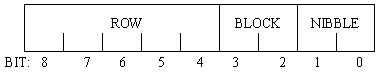
FIGURE 3.21: ADDRESS PARTITIONING
ON CACHE RAM
On-chip, the external nine bit address is divided into three fields: row, block, and nibble (Figure 3.21).
The row field consists of five bits which are used to select from among the sixteen rows of the selected cache RAM block. The row field is distributed to each of the four cache RAM blocks where it is used to address them.
The block field is used to select which of the four cache RAM blocks are selected. When a read or write occurs through the four-bit I/O port, only one block will be selected at a time. On a write, only the selected block has its write input asserted. On a read, the block field is used as select lines for a 16 bit to 4 bit multiplexor, which has as its inputs four bits from each of the four cache RAM blocks. When the 64-bit port is used for a write, all four blocks have their write lines asserted, and when it is used for a read, the block field is still used to select a block to be presented to the 4-bit dataout bus.
The nibble field selects from the four available nibbles
within each cache RAM block. Each cache RAM block contains multiplexors
which enable it to output any selected nibble to the block select
multiplexor. In addition, each cache RAM block contains four individual
write lines, one for each nibble, enabling a write to be performed
into any nibble, byte, or half-word. The logic which handles the
decoding of the nibble and block fields into individual block
select and write control lines is located in the portion of the
chip marked "Addressing Logic" in Figure 3.19.
The cache RAM critical path was simulated using SPICE, an analog circuit simulator, using capacitances extracted using Quickcap, a three-dimensional capacitance extractor, and the Compass VTITools two-dimensional capacitance extractor.
Critical capacitances within the cache RAM block were extracted
with Quickcap, and SPICE simulations were performed to confirm
that the RAM block should have an access time of 450 ps. In addition,
the complete RAM critical path from address pad I/O to data out
I/O was simulated in Spice using extracted interconnect capacitances
and resistances to assure an net access time of 750 ps.
The cache RAM is 6.703 mm wide and 9.347 mm high. The majority
of the on-chip circuitry is dedicated to the basic RAM functionality
and to the I / O pads - the testing and control circuitry represent
a small fraction of the transistors count. Table 3.6 is a breakdown
of the transistor usage on the cache RAM chip by circuit.
| Devices | ||
| I / O | ||
| Testing (not including latches) | ||
| Testing: Rotator and Counter | ||
| Testing Buffers | ||
| Testing latches | ||
| Multiplexing / Distribution | ||
| Address decoding | ||
| RAM blocks | ||
| TOTAL |
Table 3.6 illustrates that the majority of the non-RAM block device usage in the cache RAM is dedicated to I / O and testing logic. Since the testing logic in the core CPU alone requires nearly 600 devices, as well as the inclusion of the four-phase generator, it is estimated that implementing the testing scheme described in Chapter 4 on the cache RAM saved 600 devices in control logic alone, with additional savings realized by not latching the L2 I/O pads.
Power usage is concentrated in the four 16-bit RAM blocks and the pad I/O. Each bi-directional pad has two current trees, one at 8 mA and one at 1.5 mA. Each standard driver uses a single 8 mA tree while each receiver uses a 1.5 mA tree.
The drivers use more current in order to provide a larger voltage
swing on the multi-chip module (40 mV) than on-chip (25 mV) in
order to combat noise and voltage droop.
The F-RISC / G system contains two cache controllers: one each for the data and instruction caches. Each of these chips is responsible for handling all communications between the core CPU and the cache RAMs in the primary caches, as well as the secondary cache and I/O devices.
Although the responsibilities of the two cache controllers differ
slightly, it was decided to design a single, configurable controller,
due both to the cost and time required to design an extra chip;
the operation of the controllers in both caches is similar enough
that methods were found to minimize the penalty for using a single
chip.

FIGURE 3.22: SIMPLIFIED CACHE
CONTROLLER BLOCK DIAGRAM
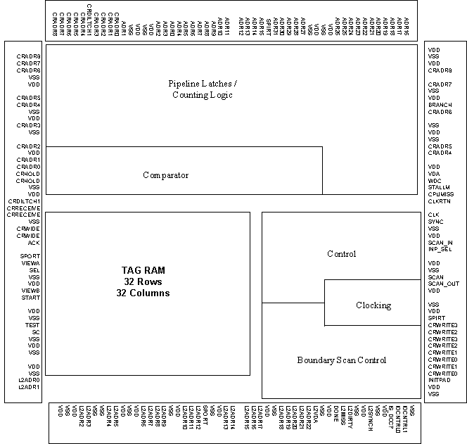
FIGURE 3.23
: CACHE CONTROLLER FLOORPLAN
The key functional components of the cache controller chip are
the tag RAM, a three stage pipeline with integrated counter, and
a comparator. The organization and interconnection of these functional
structures is illustrated in Figure 3.22, a floorplan is given
in Figure 3.23, and the final layout is illustrated in Figure 3.24.
The chip sends out 26 or 28 rather than 21 or 23 address bits
to the secondary cache in order to allow sub-block replacement
or smaller block sizes in the secondary or higher level caches.
The chip additionally includes circuitry to supply appropriate
control signals to the major functional units (see State Machine)
and circuitry which provides at-speed testing capability of unmounted
die as well as functional testing capability of mounted die.
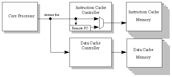
FIGURE 3.25: REMOTE PROGRAM COUNTER
The cache controller was designed for use in both the instruction and data caches. For this reason the first pipeline latch serves also as the Remote Program Counter (RPC) in the ICC configuration. Figure 3.25 shows the manner in which the two caches share a common CPU address bus and how the RPC can be loaded from this bus. If two separate cache controller chips had been designed it would have been possible to include only two pipeline latches in the DCC as at any given time only two addresses need be stored (the third always being available on the bus.) Since the hardware for the RPC had to be included, however, it was decided that it also act as a latch in order to reduce problems caused by hazards and skew on signal lines while at the same time minimizing chip configuration and initialization logic.
Also, although neither cache requires more than 23 tag bits, each tag RAM is actually 32 bits wide. This results in higher than necessary power dissipation but was deemed a reasonable design compromise because it allows the use of the same cache blocks as are used in the cache RAM. This greatly reduced design time and allows information learned from testing of one chip to be applied to both designs. In addition, two additional bits are used per row for Valid and Dirty bits.
Two data paths shown on the block diagram are critical and thus require careful optimization. The first is the 9-bit path from the ABUS, through the master of pipeline latch 1, and out to the cache RAMs.
The second critical path is the MISS
generating circuitry. This path requires reading an address from
the ABUS, addressing
and reading the tag RAM, performing the tag comparison, and driving
the results out of the pad..
The most obvious way to design the cache controller state machine would be to consider the contents of the three pipeline latches and conditions represented by those contents and assign states appropriately. For example, if the address in pipeline latch 1 causes a LOAD miss without a copyback, the state machine would enter a "LOAD miss without copyback" state.
This type of state assignment is a poor choice for several reasons. First of all, many of the "states" assigned using this method would be nearly identical. For example, regardless of whether a LOAD or STORE copyback is taking place, the operation is nearly identical (except for the values of write lines at certain times). Secondly, each "state" would encompass a series of steps during which control lines must change with each step, essentially similar to microcoded operation.
By analyzing the functional blocks in the cache controller and determining when their control lines and inputs must change value, it was possible to break any possible cache transaction into a small number of steps. Each step represents some change in control lines or a clocking of the pipeline.
Wherever possible, control signals derive from the contents of the pipeline registers rather than the state, thus further reducing state machine complexity.
Extreme caution was taken to ensure that critical control signals emanating from the state machine are stable. This required making state assignments carefully, and, in some cases, clocking control lines.
Figure 3.26 shows a state diagram for the cache controller. System
initialization forces the state machine into the READ state. Until
an acknowledged miss occurs the state machine will stay in the
READ and WRITE states, LOADing
and STOREing data as
required. When the comparator determines that a miss has occurred,
the state machine is not made aware of it. The MISS
signal is sent to the instruction decoder, which may acknowledge
it by asserting STALLM.
Only once the STALLM
is received does the state machine undergo a transition to the
MISS state. This greatly simplified the handling of unacknowledged
misses.

If the appropriate ACK signal is received, the state machine proceeds from the MISS state to the WAIT state. It is in the WAIT state that tag RAM updates, copyback, and loads from the secondary cache take place. In order to avoid incorrect modification of the tag RAM if it was the other cache that caused the stall, if a STALLM but no ACK is received, the state machine skips the WAIT state entirely and proceeds directly to the RECOVER state. Otherwise the state machine proceeds to the RECOVER state upon receiving the L2DONE signal, which notifies the primary cache that any transaction with the L2 cache is complete.
The WRITE state is used for the second half of a STORE operation. The tag RAM access and data read that occurs during the first half of a STORE occurs in the READ state. If WDC was set when the address was received by the cache, then the state machine proceeds from the READ state to the WRITE state.
The STALL state is used to allow the cache subsystem to wait for the CPU to recover from the stall and to provide a harmless state for the cache that didn't cause the stall to wait in while the cache that missed finishes its operation.
From the STALL state the state machine proceeds either to the READ or WRITE state depending on whether a LOAD or STORE was in the middle of being read from the bus when the stall occurred.
In order to get this to work properly, a trick called a "double-shuffle" needs to be performed by the pipeline when a STORE is to take place. A STORE requires two cycles since it is necessary to both read from and write to the cache in a copyback design. During the first cycle the CPU puts the address and data out on the appropriate buses, and asserts the WDC and VDA signals.
During the second half of the cycle, the VDA signal is de-asserted, and the contents of the address and data buses are unknown. The WDC signal is de-asserted.
A double-shuffle occurs when the cache controller sees that WDC has been asserted. Rather than grabbing the invalid data that will be available during the next cycle, the pipeline is clocked again during the first cycle of the STORE. This results in the first two pipeline registers each containing identical data.
The first register will have been loaded from the READ state,
so a tag RAM read takes place. The second register will have been
loaded from the WRITE state, so, assuming no miss occurs, a tag
RAM write will take place. In order to simplify later operations
in the event of a miss, the WDC
field in the trailing pipeline register is flipped from a 1 to
a 0. This allows the use of this bit of the latch to store state
information.
The cache controller contains a pad, IS_DCC?, which is used to enable the chip to be configured for either the instruction or data cache controller. For data cache use the signal is asserted by hardwiring it on the MCM.
Additionally, when the chip is intended for the data cache, the BRANCH pad should be asserted by hardwiring it on the MCM; the ICC will have the BRANCH signal asserted by the instruction decoder whenever a branch is to occur. This signal is used to determine whether the first pipeline stage (the remote program counter) is loaded or counts.
Since it is impossible to perform a STORE
into the instruction cache, the WDC
line must be hardwired low. In addition, the instruction cache
must retrieve an address on every cycle, so VDA
should be tied high.
Like the instruction decoder and datapath chips, the cache controller uses an on-chip four-phase clock generator to create four non-overlapping 250 ps clock phases from an externally supplied 2 GHz actively de-skewed clock.
In order to support the de-skew system and ensure that phase 1 on each of the clocked chips occurs at the same time, a particular clock start-up sequence is required for each of the chips. The external high speed clock is started while a SYNC signal is asserted to each of the de-skewed chips. The SYNC signal is de-asserted at all chips simultaneously, causing all four-phase generators to assert 1.
In order to synchronize the behavior of all chips, simulations were performed with all inputs and outputs timed relative to the four-phase clock at the outputs of the four-phase generator. Care was taken to assure than all chips have similar loading on the four-phase generator so that the "reference phase 1" occurred simultaneously across the MCM. After parasitic interconnect resistance was factored into the back-annotation, however, it was found that nearly all clocks were delayed by approximately a phase.
Since all clocks were delayed by nearly the same amount, it was
decided to re-reference the clocks so that the simulations showed
phase 1 to be occurring when the four-phase generator was actually
outputting phase 4.
The cache controller chip is 8.365 mm high and 9.472 mm wide.
| Devices |
| |
| I / O | ||
| Write byte decoding | ||
| Tag RAM blocks | ||
| Testing logic | ||
| Control | ||
| Pipeline and RPC | ||
| Clock distribution | ||
| Comparator | ||
| TOTAL |
Table 3.7 shows an approximate device usage breakdown for the
cache controller chip. As in the cache RAM, a large percentage
of the power is dissipated in the RAM blocks and the I/O pads.
| Devices | ||||
| Power (mW) | ||||
| Area (mm2) |
Table 3.8 compares the critical features of the F-RISC / G chip set. Despite being designed by different people, all of the chips are seen to be similar in size, area, and power dissipation. The cache controller and datapath chips are seen to be of comparable complexity (were the unnecessary columns removed from the tag RAM block this would be even more the case), while the cache RAM and instruction decoder, while being quite different in nature, are similar in size and complexity. This comparison suggests that it might be worthwhile in future designs to move some of the functionality of the cache controller into the instruction decoder.
As the F-RISC/G prototype is partitioned, inter-chip communications
becomes an important issue. Large fractions of the cycle time
on are consumed by communication between chips. Each off-chip
communication entails a driver and receiver delay (I/O delay)
as well as an MCM time of flight delay. Rise time delays and skew
must be considered as well.

FIGURE 3.27: LOAD CRITICAL
PATH COMPONENTS
Figure 3.27 shows a breakdown of the components of the LOAD critical
path in the data cache, assuming that the Byte Operations chip
is present. As can be seen, off-chip communications accounts for
over 40% of the critical path. This is a unique design space that
required special attention throughout the design process. Interestingly,
these numbers are similar to those for the F-RISC/G adder critical
path, as shown in Figure 3.28 adapted from [Phil93].

FIGURE 3.28: COMPONENTS OF
ADDER CRITICAL PATH (ADAPTED FROM [PHIL93])
Figure 3.29 illustrates the communications that occurs with the primary data cache. As can be seen from this block diagram, the primary cache communicates with the secondary cache, the datapath, and the instruction decoder.
Figure 3.30 shows that the primary instruction cache also communicates with all of the core CPU chips as well as the secondary instruction cache.

The communications to and from the cache may be divided into
datapath and control signals. The primary (L1) cache as a whole
communicates with the four datapath chips, the instruction decoder,
and the secondary (L2) cache. Within each primary cache (instruction
and data), the cache controller also communicates with the eight
cache RAMs.

FIGURE
3.30: INSTRUCTION CACHE COMMUNICATIONS
Table 3.9 lists the communications signals sent from the core
CPU to the primary cache. Aside from an address and data, the
CPU also sends out several handshaking and control signals. These
signals inform the caches of stalls and determine whether a Load
or Store is to take place.
| Signal | Width | From | To | Description |
ABUS | 32 | DP | DCC, ICC | Word (Instruction cache) or Byte (Data cache) address. Shared by both caches. |
WDC | 1 | ID | DCC | Signals data cache to perform store. |
STALLM | 1 | ID | DCC, ICC | Signals both caches to stall. |
ACKI | 1 | ID | ICC | Signals instruction cache that it has caused a stall. |
ACKD | 1 | ID | DCC | Signals data cache that it has caused a stall. |
VDA | 1 | ID | DCC | Address on bus is valid for data cache. |
IOCNTRL | 3 | ID | DCC, ICC | Flush / Initialize / Write alignment |
BRANCH | 1 | ID | ICC | Instruction cache should set RPC to address on bus. |
DATAOUT | 32 | DP | DRAM | Word of data to be stored in data cache. |
The IOCNTRL lines are a 3 bit field that is part of the LOAD and STORE instructions, and are sent to both cache controllers. These bits are used to inform the caches when the system startup routine is complete, and to inform the data cache in the event of aligned byte or half-word writes. The meaning of the control bits are as shown in Table 3.10.
As the data cache receives a byte address from the datapath (unlike
the instruction cache, which uses word addresses), support is
provided using IOCNTRL
to allow reads and writes to any byte, half-byte, or word in the
processor's address space. To read a non-word-aligned byte or
half-byte, however, requires the presence of the Byte Operations
chip on the MCM. Non-word aligned word-fraction Store support
is provided in the DCC.
| Meaning | |
| Read or write entire word | |
| Read or write half-word | |
| Read or write byte | |
| Force a miss on this address | |
| Co-processor support |
In order to prevent the need to design two different cache controllers,
the cache controller chip is designed internally to handle either
word or byte addresses. On the DCC, ABUS[2],
the word address, must be wired to the pad ABUS[0].
Similarly, each bit on the bus is wired to the pad corresponding
to its position in the word address. The two low order ABUS
bits (byte address) are wired to the high order pads (See Figure 3.31).
The controller chip knows to ignore these two bits when handling
tags and presenting addresses to other chips, and uses them only
when writing into the RAMs.

FIGURE 3.31: ABUS PARTITIONING
| Signal | Width | From | To | Description |
MISSI | 1 | ICC | ID | A miss has taken place in the instruction cache. |
MISSD | 1 | DCC | ID | A miss has taken place in the data cache. |
INSTRUCTION | 32 | IRAM | ID | 32 bit Instruction |
DATAIN | 32 | DRAM | DP | Word of data for the datapath. |
Table 3.11 lists the signals sent from the cache to the CPU. These consist mostly of requested data, but also include signals to inform the CPU that a miss has occurred and the requested data will not be available in time.
The handshaking between the CPU and the cache is described briefly in [PHIL93]. Careful simulation and analysis of the completed instruction decoder and datapath netlists were performed to fill in some details of the interface which were not fully described by Philhower.
Each cache behaves a little differently. In the instruction cache, the Remote Program Counter (RPC) on the ICC will produce an address once per cycle, between phases 2 and 3. This address will be the same as that contained in the datapath's Program Counter (PC) except in the event of a taken Branch. When a Branch is not to take place, the instruction cache must produce the required instruction at the instruction decoder by as early as between phases 3 and 4 of the following cycle. If the proper instruction is not stored in the cache, the MISSI signal must be asserted by that time.
In the event of a taken Branch, the CPU must put the branch target address on the ABUS between phases 1 and 2. Simultaneously, the BRANCH line must be asserted in order to inform the cache that a Branch is to take place.
Between phases 2 and 3, when the RPC would normally increment, the new address will instead be loaded into the counter. From this point on, the cache handles the address identically to an RPC-generated address.
The data cache, when performing a LOAD, behaves similarly to the instruction cache during a BRANCH. The datapath puts out an address between phases 1 and 2. The WDC line is low, indicating a Load is to take place, and the VDA line is high, indicating that the address on the bus is valid. The cache controller loads the address and returns either the requested data, if it is in the cache, or asserts MISSD.
The data cache has 2250 ps from the time the instruction decoder
starts to drive its address I/O drivers (or 2110 ps from the time
the address is actually on the bus) to return the requested data
on a read hit. The instruction cache requires most of the instructions
in 2100 ps, but some sooner (Table 3.12).
| Critical Path | Time |
| Data cache | 2250 ps |
| Instruction cache (bits 3-7) | 1850 ps |
| Instruction cache (remaining bits) | 2100 ps |
In the event of a STORE the WDC line is merely asserted while the address is on the bus, and the datapath puts the data to be written on the DATAOUT bus. The data cache will either store the data, or, if the cache line is occupied by the wrong address, inform the CPU by asserting MISSD. As a successful STORE requires two cycles (one to read the tag RAM and one to write to it), a STORE may not be followed immediately by any other cache operation (LOAD or STORE).
Once the CPU is informed of a miss, it may react in two ways. In the event the cache transaction which caused the miss has been flushed by the CPU, the instruction decoder will fail to assert the ACK and STALLM signals. The caches will then ignore the miss, and move on to the next valid cache transaction.
In the event the CPU has not flushed the offending cache transaction (and thus requires that it be completed), the instruction decoder will send both cache controllers the STALLM signal, and will assert the appropriate ACK signal. Interestingly, the ACK signals are clocked while the STALLM signal is asynchronous. As a result, the caches will receive the STALLM signal near phase 1, while the ACK will not arrive until around phase 3.
Upon receiving the STALLM and ACK signals, the cache which missed will communicate with the secondary cache as necessary to complete the transaction. When the transaction is complete and the appropriate data has either been stored in the cache or put on the DATAIN or INSTRUCTION buses, the offending cache lowers its MISS signal, informing the CPU that it can enter its stall recovery cycle.
| Signal | MCM Length (mm) | Delay (ps) |
ABUS | 21 | 170 |
WDC | 21 | 170 |
STALLM | 26 | 190 |
ACKI | 17 | 140 |
ACKD | 25.5 | 190 |
VDA | 21 | 170 |
BRANCH | 15 | 135 |
DATAOUT | upper path: 22lower path: 27 | 170
200 |
MISSI | 18 | 150 |
MISSD | 25 | 185 |
INSTRUCTION | fast bits: 13slow bits: 24 | 120
170 |
DATAIN | upper path: 22lower path: 28 | 170
200 |
Table 3.13 lists the line lengths and associated delays for communications between the CPU and the primary cache. The line length figures are based on work performed by Atul Garg as part of his doctoral research. In order to determine these line length figures, Garg performed a hand route of the entire MCM.
The delay figures are based on a dielectric with =2.67, which
translates to a time of flight on the MCM of 5.44 ps/mm. An additional
50 ps per line was allowed for rise time degradation and slack.
| Signal | Width | From | To | Description |
CRABUS | 9 | CC | RAM | 5 bit row address and 4 bit word address. |
CRWRITE | 4 | DCC | DRAM | Write / . |
HOLD | 1 | CC | RAM | Prevent RAM outputs from changing.. |
INLAT | 1 | CC | RAM | Allow 4-bit data input to pass through input latch. |
CRWIDE | 1 | CC | RAM | Select wide input path (64 bit) for write from L2.. |
CRDRIVE | 1 | CC | RAM | Control bi-directional L2 bus. |
The primary caches each consist of a single cache controller
chip and eight cache RAM chips. While there is no inter-cache
communication (i.e. the instruction and data caches do not communicate
with each other), there is extensive communication between each
cache controller and its associated RAM chips.
| Signal | From | To | Description | |
L2ADDR | CC | L2 | 23-bit line address. | |
L2DONE | L2 | CC | Indicates that the L2 has completed a transaction. Any data L2 places on the bus must be valid when this is asserted. | |
L2DIRTY | CC | L2 | Indicates that the L2 will be receiving an address to be written into. | |
L2MISS | CC | L2 | Indicates that the address on L2ADDR is needed by the CPU. | |
L2VALID | L2 | CC | Indicates that the current data in the cache row specified by the cache tag currently being transacted is correct. De-asserted by L2 during TRAP. | |
L2SYNCH | CC | L2 | A 1 GHz clock used for synchronizing with L2. | |
L2VDA | CC | L2 | The address currently on L2ADDR is valid. |
Table 3.14 lists communications lines between the cache controllers and RAMs. The controllers send out addresses to the RAMs just after phase 3. The settings of the control lines are determined by the type of operation being performed and the state of the cache.
The CRWRITE line is used to write into the cache RAMs. The CRWIDE line is used to toggle between the 4-bit per RAM CPU data path and the 64-bit per RAM L2 data path. The CRDRIVE line is used to control the bi-directional drivers / receivers used on the RAMs for communicating with the L2 cache.
The HOLD and INLAT signals are used to latch the RAM 4-bit data outputs and inputs, respectively. These latches allow the RAMs to be pipelined.
The lengths of each of these lines or buses is less than 45 mm,
for an estimated flight time of 300 ps.
Table 3.15 enumerates the signals used for communication between the primary and secondary caches.
As much freedom as possible was given to the designer of the secondary cache while still assuring that the "usual case," the LOAD hit, is optimized. As a result of uncertainty as to the exact design of the L2 cache and the fact that the secondary caches do not share the synchronized clock used by the primary caches and core CPU, the timing requirements of the secondary caches are very specific.
Each cache controller will send out a 28 bit cache line address as soon as it is received from the CPU. This is done to allow the L2 cache to read its tag RAM simultaneously to the L1 cache. The cache controller will assert L2DIRTY as soon as it completes its tag RAM access if the accessed line is dirty. The L2 will not receive the address as stored in the primary caches tag RAM until later, however, and only if it is required (that is, a stall occurs.)
The cache controller asserts L2MISS only if a miss occurs and the CPU acknowledges the miss. Whenever the address on the L2ADDR bus is valid, L2VDA is asserted.
Since the secondary caches do not have a synchronized clock, the L2SYNCH signal is used to inform the secondary caches that valid data is on the control and address lines. When the L2SYNCH signal goes high the data on the L2 communications lines is valid. It remains so for approximately 500ps. If the MCM routing is done carefully, it may be possible to assure that the L2 communications signals are valid for as long as L2SYNCH is asserted.
The L2DONE signal is asserted by the L2 to indicate that it has performed the requested operations, both modifying its RAMs as appropriate and placing requested data on the bus. Any data being sent by the L2 must be on the bus for 750ps prior to L2DONE being asserted.
In the event that the primary cache has to perform a copyback, the secondary cache will first receive the address (originating from the CPU and passing through the primary cache controller) that caused the copyback, along with the L2DIRTY signal and the data to be copied back, which should be latched at that point. Two more addresses will appear on the bus to the L2 (although they may or may not be valid), followed by address that had been stored in the tag RAM (the address of the data being copied back).
This "out of order" execution, in which the L2 may
perform the read before the write on a copyback from the primary
cache, allows maximum flexibility for the secondary cache designer
(for example if two port RAM is available.)

FIGURE 3.32: MCM LAYOUT
The F-RISC / G processor is designed to mounted on a thin film Multi-Chip Module (MCM). Four datapath chips, the instruction decoder, the two cache controller chips, and the sixteen RAM chips will all be mounted on this MCM. In order to achieve the timing necessary to operate the processor with a 1 ns cycle time, the chip placements on the MCM had to be carefully considered.
Figure 3.32 shows the placement of the core CPU and primary cache
chips on the MCM. The placement of the datapath (DP) and instruction
decoder (ID) chips is determined by the constraints of the CPU
adder critical path. [Phil93] provides an analysis of this aspect
of the MCM floorplan. [Phil93] reports that the worst case communication
between the core processor chips is the "daisy-chain"
broadcast from the instruction decoder to each of the four datapath
chips. Due to the layout of the instruction decoder, the signals
to be broadcast must often be driven from the side of the chip
farthest from the datapath chips. The sizes of all of the F-RISC
/ G core and cache chips are given in Table 3.16. These chips
are all significantly larger than the 8 mm x 8mm size which Philhower
assumed in his calculations, due mostly to the late inclusion
of terminating resistors in the pads. These restrictions severely
constrained the placement options for all of the cache chips on
the MCM. In low device-integration, partitioned designs, the placement
of the core CPU chips will, as a rule, constrain the placement
of the cache chips in this way, so long as speed is the primary
concern.
| Chip | |||
| Datapath | |||
| Cache RAM | |||
| Cache Controller | |||
| Instruction Decoder |
In the cache there are several critical and slightly sub-critical
paths which needed to be carefully considered when placing the
cache chips on the MCM.

FIGURE 3.33: ADDRESS BROADCAST
TO CACHE CONTROLLERS
Since the datapath must frequently send addresses to both cache
controllers (Figure 3.33), it is desirable to locate the cache
controllers proximally to the datapath chips. The instruction
decoder will frequently receive data from the instruction cache
RAMs, and the datapath chips will each receive data from a pair
of data cache RAMs, further constraining the placement (Figure 3.35).
Finally, the cache controller must broadcast addresses and control
information to the cache RAMs (Figure 3.34). The layout shown
in Figure 3.32 was arrived at after several iterations based on
improved information regarding the MCM characteristics and regarding
chip dimensions and pad placements and was the work of myself
and Atul Garg.
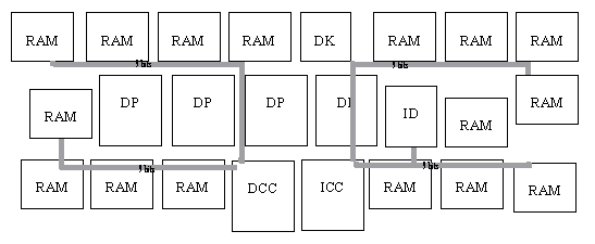
FIGURE 3.34: ADDRESS BROADCAST
TO RAM'S

FIGURE 3.35: RESULTS FROM CACHE TO
CPU

FIGURE 3.36: GE-HDI MCM CROSS-SECTION
The primary candidate for the F-RISC / G interconnect design
is the General Electric "High-Density Interconnect"
package (GE-HDI) [Hall93,GE95]. The GE-HDI package features a
ceramic substrate with recesses into which die are mounted (Figure 3.36).
A tape-style routing mechanism is used.
|
|
|
| |
| Dielectric | Parylene | Parylene | Kapton | Polyimide |
| Propagation velocity | 0.18 mm/ps | 0.18 mm/ps | 0.16 mm/ps | 0.18 mm/ps |
| Chip attachment | C4 | TAB | GE-HDI | GE-HDI |
| Chip spacing | 1 mm | 3 mm | 1 mm | 0.1 mm |
| Shortest CPU broadcast [Phil93] | 156 ps | 200 ps | 175 ps | |
| Average CPU transfer
[Phil93] | 200 ps | 244 ps | 225 ps | |
| Shortest CPU broadcast | 176 ps | 224 ps | 197 ps | 156 ps |
| Average CPU broadcast | 222 ps | 270 ps | 249 ps | 198 ps |
Table 3.17 lists some of the alternative packages being considered for use with F-RISC / G. The primary CPU critical path is the "average CPU broadcast," which must be completed in 250 ps (one phase). Two sets of figures for each broadcast are given. The smaller figures represent data from [Phil93], which assumed that the die were 8 mm wide. It was later determined that the terminating 50 resistors required at the end of each daisy-chained net needed to be included in the die pad cells. As a result, the chip sizes increased, despite the recent modification of all of the chips to take advantage of a third metallization layer which Rockwell made available. The higher broadcast numbers supplied in the table take the new chip sizes into account.
Dielectric constants for Parylene range as low as 2.38 for Parylene-F [Dabr93] (2.65 for Parylene-n at 1 MHz [Beac88] was assumed in this table).
The last column in the table represents a recent improvement
in G.E.'s HDI package. As illustrated in the table, G.E. claims
to have greatly reduced the inter-chip spacing, while incorporating
polyimide to provide a better dielectric constant.
The F-RISC/G CPU is designed with rudimentary support for virtual
memory. Specifically, control and communications lines are provided
to enable the caches to signal the CPU in the event of a page
fault, as shown in Table 3.18.
| Signal | Width | From | To | Description |
| TRAPD | Cache | CPU | Data cache page fault | |
| TRAPI | Cache | CPU | Instruction cache page fault | |
| I1, I2, I3 | Cache | CPU | Status lines sensed by PSW | |
| O1, O2, O3 | CPU | Cache | Status lines controlled by PSW |
The word addresses supplied by the CPU to the instruction cache and the byte addresses supplied by the CPU to the data cache are "virtual addresses" in that they refer to a location in the CPU's memory space without regard to their actual presence in physical memory. The CPU doesn't care where a particular virtual address maps to, as long as when data is requested from that address it is available.
Since the virtual instruction space is 232 words in size and the data memory space is 230 words in size, it is unlikely that the amount of physical RAM available in main memory will span the entire virtual memory space. In a typical virtual memory system, hardware and software is provided to allow the virtual memory to be divided into pages each of which may exist either in physical memory or on a secondary storage device, such as a disk drive. When the CPU requests a transaction to an address which is in a page not currently in physical memory, a "page fault" occurs, and the page which is needed is loaded from secondary storage, replacing another page already in physical memory if necessary. Since the amount of time necessary to access the secondary storage device, transfer the existing memory page to this device, locate the required page on the disk, and retrieve it back into memory is extremely long compared to the CPU cycle time, it is desirable for the cache to inform the CPU of the problem and allow the CPU to proceed with other instructions while the page swap occurs, if possible. This is typically performed by the operating system which will "context switch" to another waiting, unrelated process.
The hardware necessary to convert the virtual address into a physical address is similar in complexity and design to the cache hardware. A RAM is used to keep track of which pages are currently in physical RAM, and a comparator is used to determine whether the page currently stored in a particular "page frame" is the desired page. Due to the hardware cost of such a system, the virtual to physical address translation can not occur in the primary cache.
Instead, it is expected that some higher level of memory, perhaps the level just before main memory, will handle the translation of virtual addresses into physical addresses. When a page fault occurs at this level of memory, the CPU is informed via the TRAPD or TRAPI signal. The CPU then handles the interrupt by branching to the appropriate trap vector. It is presumed that the operating system has installed code at the appropriate trap vector to handle page faults. The caches will send "DONE" signals all the way down to the primary cache, which will recover from its stall and lower the MISS line as if it had the correct data. The cache must then be re-validated through a flush of the incorrect address. The CPU will lower the STALL and ACK in response to the primary cache lowering its MISS, and will prevent it from going high again in response to the incoming TRAP.
Specifically, it is necessary for the operating system to "flush"
the lower level caches in the event of a page fault. The highest
level of cache (the level containing the address translation hardware)
will signal that a page fault has occurred. The operating system
will then force each level of cache to replace its contents with
the contents of the page just loaded at the highest level of cache.
The primary cache will mark the tag RAM row containing the tag
of the address which caused the trap as "invalid." Any
future references to that tag will thus automatically generate
a miss, and result in the proper data being accessed from main
memory.
| Reset | |
| System error | |
| Data cache page fault | |
| Arithmetic trap | |
| Software trap | |
| Instruction cache page fault | |
| Device interrupt | |
| User interrupt |
Typically, the CPU, upon receiving the TRAP, will perform instructions which don't involve the memory location which page faulted, and, when the page is finally available, will re-issue the request. The CPU contains pipeline stages which enable it to re-issue a LOAD or STORE which result in a page fault.
The exact behavior of the CPU in response to a memory page fault depends on the contents of the CPU pipeline and the state of the caches at the time the page fault occurs.
LOADs and STOREs are the only instructions which have not completed by the time they enter the CPU's DW stage. In order for these memory-accessing instructions to complete, the DW stage must complete without being flushed. If a LOAD or STORE is in the DW stage when an interrupt or trap occurs the processor will determine whether or not to complete the access based on whether the instruction can be completed without invalidating the register file or cache RAM. Table 3.19 lists whether the CPU will abort the instruction in the DW stage for each possible interrupt or trap. If the instruction is aborted, the history registers are stalled and the address of the LOAD or STORE is thus preserved.
If the instruction in the DW stage is aborted, it must be re-issued following the completion of the interrupt recovery.
In the F-RISC / I system, which has a considerably slower cycle time and thus can afford more delay in the cache critical path, there is assumed to be a translation lookaside buffer in the primary cache [Tien95]. A TLB is used to, in effect, cache translations between virtual and physical addresses.
The operation of the TLB is essentially identical to the cache. The "tag" is a portion of the virtual address, while the "data" is the physical page-frame number.
The advantage of implementing a TLB is that performing a translation when the address is stored in the TLB is significantly faster than loading the page table from main memory.
One problem is that, in general, the virtual address must be passed through the TLB to produce a physical address which can be used to access the cache. This greatly increases the cache access time. In F-RISC / I, this can be avoided by using the offset within the page to access the cache (the offset with the page obviously does not require translation). The cache access can then proceed in parallel to the TLB access. If the block size is no bigger than the size of the cache, then there would be no penalty for accessing the TLB in parallel.
Implementing a TLB would, however, increase MCM path delays on
critical signals, as well as increase the power which the MCM
needs to dissipate, so no TLB was included in the primary cache
on the F-RISC/G MCM.
As mentioned earlier, the cache memory hierarchy has its own
critical paths. The most critical of these is the path from address
generation at the CPU to data reception by the CPU. The constraints
on this critical path are given in Table 3.12.

FIGURE 3.37: DATA CACHE TIMING -CLEAN LOADS
Figure 3.37 is a timing diagram of data cache LOAD operations. This timing diagram is based on the back-annotated (post-route) netlists for the cache controller, instruction decoder, and datapath chips. The vertical timing lines represent synchronized clock phase 1. Slightly after phase 1 of the first cycle, the CPU puts address (20)hex on the ABUS (Table 3.20).
| Signal | Delay from phase 1 |
| ABUS | |
| WDC | |
| VDA | |
| BRANCH | |
| DOUT |
It arrives at the data cache controller during phase 2 where it passes through the master of pipeline latch 1. The WDC and VDA lines are stable prior to the address. On the DCC, the tag RAM receives its inputs (address and data) from the master of pipeline latch 1, while the slave is used to feed the comparator. The tag RAM read access time is approximately 500 ps.
As shown in the figure, at the start of the next cycle the CPU
puts out address (30)hex on the ABUS.
Both addresses will result in hits since we are assuming that
the entire tag RAM has been initialized to 0's.
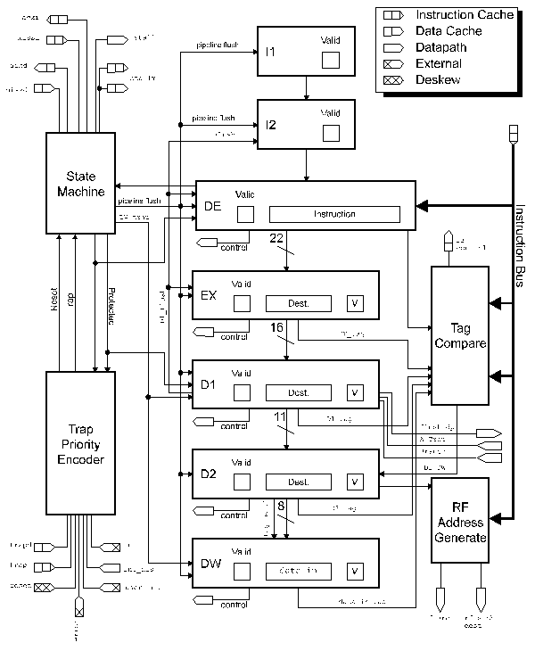
FIGURE 3.38: INSTRUCTION DECODER BLOCK DIAGRAM
The next address the CPU puts on the bus is (10000020)hex. This translates into cache line 2, tag (100000)hex. Since line 2 of the tag RAM holds a 0, this will result in a miss. The miss to the CPU will be asserted at the CC pads by phase 3 of the cycle following the cycle in which the address was put on ABUS. The CPU will receive the miss by the start of phase 4.
In response to the miss, the instruction decoder is expected to respond asynchronously with a STALLM, and then with an ACKD, except if the instruction which caused the miss has since been flushed. The STALLM should be received during the following phase 1. Figure 3.38 is a block diagram of instruction decoder operation. As can be seen, the TRAP signals from the caches are prioritized along with other trap conditions, and passed to a state machine which produces the ACK and STALLM signals.
Upon receiving the STALLM, the CC goes into its miss operations. It should be noted that the cache will go into its miss behavior upon receipt of STALLM regardless of whether an actual miss has occurred. This allows both caches to remain synchronized when only one misses (due to the ability of the non-"guilty" cache to skip the WAIT state).
When a clean miss occurs during a LOAD the primary cache must write the proper tag into its tag RAM and fetch the requested data from the secondary cache. In the F-RISC cache, the data is also stored in the primary cache while it is being sent to the CPU.
The cache controller chip prepares for the reception of data from the L2 cache and for the modification of the tag RAM by performing a pipeline rotation prior to entering the WAIT state. While in the WAIT state, the address requested by the CPU remains in pipeline latch 1 (the A stage). This address is used to address the tag and cache RAM's, and to supply the tag to be written into the tag RAM.
The cache controller signals the L2 that data is required by asserting the L2MISS signal subsequent to receiving the STALLM signal from the CPU. The cache controller will then stall the cache in the WAIT state indefinitely, awaiting the assertion of the L2DONE signal. Due to the asynchronous nature of this communication the speed of the L2 cache is unimportant for proper cache operations except in so far as it impacts on overall system speed.
While awaiting the data from the L2 cache in the WAIT state, the cache RAMs are set to WRITE from their wide data ports. When the data finally arrives from the secondary cache, it will be written into the cache RAMs. Eventually, the contents that are being written into the RAM's will appear on the RAM CPU output port. For this reason the L2DONE signal must lag the incoming data by at least the amount of time it takes for the RAM's to write in the data and let the appropriate word filter through to the outputs.
After the cache RAMs supply the data to the CPU, the only remaining task for the cache is to inform the CPU that the data is available and to re-synchronize with the CPU's pipeline.
The cache controller will perform an additional pipeline rotate
to re-examine the address that followed the address which caused
the miss (address (50)hex). The MISS
line is de-asserted to inform the CPU that the appropriate data
is now available. The CPU latches the data if appropriate, and
then puts the address which had succeeded the missed address back
on the bus. The cache controller will, however, use retrieve the
address from its pipeline latches. This will occur in the RECOVER
state.
STORE [0+20]=R2 ; store register 2 into address 20hex
ADDI R3=0+FE20 ; the add instructions are used to
ADDI R3=0+3FFF /LDH ; assemble 3FFFFE20 as the
destination for the LOAD
LOAD R1=[0+R3] ; put the contents of 1024 into R1
FIGURE
3.39: SAMPLE LOAD COPYBACK CODE FRAGMENT
The situation is more complicated if the cache row corresponding to the cache access is marked as dirty. If a miss occurs and the cache row is dirty, the primary cache must send the current contents of that row to the secondary cache before overwriting it with the data requested by the CPU.
Figure 3.39 is an example of code that would result in this condition. The first line of code stores the contents of register 2 into cache row 2 (the row is calculated by bits 4 through 8 of the address). The corresponding tag would be 0, and the dirty bit would be set to indicate that the CPU has changed the contents of this address and that the higher levels of memory are out of date.
The two ADDI instructions are used to set register 3 to 3FFFFE20 (the use of two instructions is necessary since no F-RISC instructions accept 32 bit literal values). Finally, the LOAD instruction should fetch the contents of 3FFFFE20 into register 1.

FIGURE 3.40: DATA CACHE TIMING - LOAD COPYBACK
3FFFFE20 corresponds to cache row 2 and tag value 1FFFFF. Since row 2 previously held tag 0, a miss will occur. Since the dirty bit for row 2 is set, a copyback must first take place.
Figure 3.40 is the timing diagram for this example. The STORE request is received by the primary cache at time 9375. In order to show the worst case, only one cycle of latency is allowed on this timing diagram between the STORE and subsequent LOAD. The LOAD request is received at time 11375.
By time 12460 the cache controller has determined that the tags do not match and that the current tag is dirty, and asserts MISS to the instruction decoder, and L2DIRTY to the secondary cache. The secondary cache will also be receiving the address 80000hex which corresponds to the address being requested by the CPU (the nine lower order bits are discarded since the secondary cache will use a block size at least as big as that of the primary cache). In addition, the secondary cache will receive the current contents of row 2 of the cache, specifically the block containing the contents of register 2. The secondary cache will have to latch this data since it doesn't yet know what address it corresponds to. The advantage of sending the address from the CPU rather than the address from the tag RAM is that the secondary cache can begin its access of the CPU requested address, thus speeding up LOADs, the most common case.
The MISS signal to the secondary cache is delayed until the CPU acknowledges the miss by asserting STALLM. Once the CPU has acknowledged the miss, the secondary cache will receive the address corresponding to what had been stored in the tag RAM, 20hex. This occurs when the cache controller pipeline rotates so as to allow a new tag to be written into row 2 (in this case 1FFFFF), and to allow the dirty bit for that row to be set to 0. The pipeline rotate also allows the RAMs to write in new data, from the L2 cache.
While in the WAIT state, the cache RAMs are set to WRITE WIDE. When the data is made available by the secondary cache, the write will take place. The bidirectional driver / receiver pads used on the cache RAMs to communicate with the secondary cache are set by the cache controller to receive whenever a WRITE is taking place. Since it takes approximately 750 ps to write into the cache controller, L2DONE must be delayed by at least that long after valid data is sent from the secondary cache.
The cache controller is responsible for delaying the data from
the cache RAMs until the datapath is ready for it, and for ensuring
that the data remain stable for as long as necessary. This is
accomplished through the HOLD
signal. Both Figure 3.37 and Figure 3.40 show the operation of
this signal. In the datacache, it is necessary to delay the data
by approximately half a cycle. If the Byte Operations chip is
present this delay is not necessary, and the HOLD
inputs to the RAMs could just be tied low.
Figure 3.41 is a timing diagram showing consecutive STORE
instructions. When a STORE
is to take place, the instruction decoder signals the cache controller
by asserting the WDC
signal. Since the signal is derived from the instruction word
and can be sent directly from the instruction decoder rather than
the datapath chips, the signal arrives a few hundred picoseconds
before the address (at time 9075 in this example).
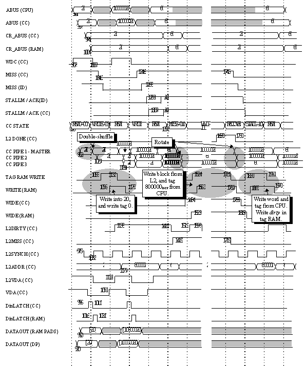
FIGURE 3.41: DATA CACHE TIMING - STORE COPYBACK
Every STORE instruction is allocated two cycles by the CPU. The second cycle is necessary because a STORE requires a read from and a write to the tag RAM.
For the first of the two cycles, the cache controller will be in the READ state. While in this state, the cache controller checks the tag RAM in order to determine whether a hit has occurred. As far as the cache controller is concerned, the first half of a STORE instruction proceeds identically to a LOAD instruction.
The cache controller latches the address from the CPU during
the first half of the STORE,
so the CPU does not have to keep the address stable for two cycles.
During the second cycle the comparator calculates the result.
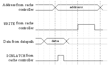
One important aspect of the STORE
operation is the latching of the data from the CPU by the cache
RAMs. The cache controller determines when the cache RAMs latch
the input data from the CPU using the DILTCH
signal. The signal is used to enable the cache RAMs to latch the
data when appropriate so that the CPU need not hold it on the
bus for two cycles. In the event of a miss, this signal is especially
important, enabling the cache RAMs to be written into several
cycles after the data was put on the bus.
STORE [0+20]=R2 ; store register 2 into address 20hex
ADDI R3=0+20 ; the add instructions are used to
ADDI R3=0+1000 /LDH ; assemble 10000020 as the
destination for the next STORE
STORE [0+R3]=R4 ; store register 4 into address
10000020hex
In order to simplify the state machine design, the WDC signal is latched by the cache controller pipeline latches. The cache controller performs a "double-shuffle" during the first half of the STORE so that two pipeline latches will contain the address supplied by the CPU. The pipeline is advanced twice during the same cycle because there is no assurance that the address will still be on the bus during the second cycle. The trailing pipeline latch will have its WDC bit flipped low, which simplifies the state machine by forcing the next state (following the WRITE state) to READ. The VDA signal is forced high during the second half of the shuffle since by that time it may have been de-asserted by the instruction decoder. By using these techniques, it was possible to reduce control circuitry, since the LOAD and STORE proceed identically, and the READ and WRITE states are identical with the exception of some write control lines.
Once again, the situation becomes more complicated if the row into which the data is to be stored contains a tag which is marked dirty. Assuming the tag doesn't match the tag of the address into which the CPU would like to perform the STORE, a copyback must occur.
Figure 3.43 gives sample code for a situation involving a STORE copyback. As in the LOAD copyback example, the initial store results in row 2 of the cache RAM being marked as dirty. In this case, the eventual STORE to location 10000020hex will conflict with the previous store. Once again, the tags will not match, resulting in a miss. Again, the dirty bit is set, causing a copyback to take place. The cache must send the secondary cache the data already in row 2 before receiving the requested block from the secondary cache and modifying the word of that block selected by the CPU.
The cache controller will receive address 10000020hex from the datapath chip at time 11375. At time 13070, the cache controller has received the STALLM from the instruction decoder, indicating that the CPU is acknowledging the miss and will stall.
The data corresponding to address 10000020hex is presumed to reach the cache RAMs around time 11500, around a half-cycle later than the address arrives at the cache controller. At time 12160, the DINLATCH signal arrives at the cache RAMs from the cache controller. The signal remains asserted for approximately 150 ps. When this signal is asserted, the input D-latches in the cache RAM pads are opened, allowing the data on the pads to reach the core. The cache RAM is therefore ready to write in the data when the address and WRITE signals arrive (in this case, this will occur several cycles later, since a copyback need take place).
The secondary cache will receive the address 80000hex, corresponding to the address sent by the CPU (with the low order bits removed) so that it can begin to look up that address. The secondary cache will also be sent the block currently in row 2, which must be latched.
Several cycles later, in the WAIT state, the secondary cache is sent the address 2, which corresponds to the address 20hex which had been stored in the cache. At that point, the secondary cache can store the data it had previously latched into the appropriate location. Meanwhile, the primary cache will set its RAMs to WRITE, WIDE, and RECEIVE in preparation of receiving the block it had been expecting from the secondary cache.
Finally, the primary cache must still store the data sent by
the CPU, and set the dirty bit appropriately. This occurs in the
STALL state.

FIGURE
3.44: INSTRUCTION CACHE MISS TIMING
The instruction cache timing is, in most respects, similar to the timing of the data cache during a LOAD. This is particularly true when a BRANCH occurs.
The instruction cache controller contains a remote program counter (RPC) which is used to generate addresses to fetch and send to the CPU. This occurs without any intervention from the datapath or instruction decoder. In the event of a BRANCH, the address is received off of the ABUS, as in the data cache.
Unlike in the data cache, it is not necessary to delay the data sent to the CPU using the HOLD signal, since the instruction cache timing is much more constrained.
When the CPU starts up, a "phantom" BRANCH to location 20hex is injected into the pipeline. Figure 3.44 illustrates how such a BRANCH might take place. As in the data cache, the target address is expected to be available at the cache controller at approximately 375 ps after "phase 1" (simulation time 9375). The actual BRANCH signal arrives approximately a phase earlier.
The primary cache will forward the address to the secondary cache as soon as it arrives. The address will be latched into the first pipeline latch's master approximately 175 ps after it arrives at the receiver pads (the delay is caused by the receiving circuitry, the primary cache's input multiplexor, and the latch gate propagation time).
The BRANCH signal is assumed to go low within 1 cycle. As a result, the RPC will be incremented to provide the next address (21hex). The RPC is constructed of four-bit ripple-carry slices with parallel carry enable. The increment has nearly a full cycle to take place before the pipeline latch is again toggled.
As soon as the primary cache has incremented the address, it is sent to the secondary cache. Of course, the lower 9 bits are stripped off, so the address being sent to the secondary cache will change only once every 16 times the RPC increments. In the example, a second BRANCH takes place (the address arrives at 11375). This time, the branch target address is FFFFFFFFhex.
The simulation assumes that cache line 1Fhex contains
tag 0. As a result, this BRANCH
will result in a miss.

FIGURE 3.45: CACHE WAIT TIMING
In the instruction cache, the only time a write occurs into the tag RAMs is during the WAIT state. Figure 3.45 shows the timing at the cache RAM when this occurs. As this diagram indicates, the WIDE signal is asserted before the WRITE signal is asserted, and is brought low after the WRITE signal goes low again. This is important because the signal which is used to control whether the bi-directional I / O pads on the RAMs are driving or receiving is a mirror of the WIDE signal. It is obviously undesirable to have two drivers (the L2 cache RAM and the primary cache RAM) driving a line simultaneously. While hardware could have been incorporated into the cache RAM to ensure that the pads always drive when reading to the secondary cache and receive when writing from the secondary cache, having a separate DRIVE signal allows more flexibility in the secondary cache design, and allows the RAMs to be used for purposes other than the F-RISC / G prototype.
The timing of the instruction cache is more critical than that in the data cache. The architecture was designed to support a byte-operations chip in the data cache; by not including it, the timing in the data cache became fairly relaxed. Table 3.12 shows that the instruction cache has only from 1850 ps - 2100 ps in which to perform a fetch, versus 2250 ps in the data cache. Bits 3-7 of the instruction word must arrive at the instruction decoder a phase earlier than the remaining 27 bits.
In order to allow bits 3-7 (the "fast" bits) to arrive
more quickly, the two RAMs which supply these bits to the instruction
decoder were placed as close to the ID as possible without increasing
the distance from the instruction cache controller.

When a cache determines that a miss has occurred and that it will not be able to satisfy the CPU's request in the time allotted, the cache controller will assert the appropriate MISS line (MISSI for the instruction cache, or MISSD for the data cache).
If the CPU determines that the request to the cache can not be flushed, it must stall, and will assert the STALLM line, which is shared by both caches.
Upon receiving STALLM each cache will move into the MISS state. At the time this occurs neither cache knows whether it is the cache which caused the stall. In order to inform the appropriate cache that it is responsible for the stall (and must perform a fetch), the instruction decoder will assert the appropriate acknowledgment line (either ACKI or ACKD).
The cache that receives both the ACK and the STALLM will progress through the normal miss cycle as previously described. The other cache will behave almost identically, but will skip the WAIT state, thus preventing any cache state information from being overwritten. This cache will skip directly into the RECOVER state, and, one cycle later, will enter the STALL state where it will idle while awaiting STALLM to be de-asserted. Since the pipeline rotate occurs only in the RECOVER state (rather than in the STALL state), the pipeline in the non-stalled cache will be in the proper state when the CPU recovers from the stall.
Figure 3.46 illustrates the timing in the data cache during a
stall caused by the instruction cache (an "instruction cache
stall"). Figure 3.47 show the timing in the instruction cache
during a stall caused by the data cache (a "data cache stall").

FIGURE
3.47: INSTRUCTION CACHE DURING A DATA CACHE STALL
One of the most important responsibilities of the cache is to enable the processor to correctly start up. When the processor is powered on, or reset, it needs to be fed the appropriate start-up instructions, and the data cache must be invalidated or pre-loaded with valid data.
When the processor is initialized, it inserts an unconditional BRANCH to location 20hex into the pipeline. It is the responsibility of the instruction cache to fetch this instruction upon receiving the BRANCH signal and the address.
Figure 3.48 illustrates the timing at the instruction cache controller
during processor start-up. The cache controller will receive the
branch request and must realize that a miss must occur, regardless
of whether the tag in the tag RAM accidentally matches the tag
of the start-up address (0). This is accomplished through coordination
with the secondary cache, since too little handshaking exists
between the CPU and the cache to enable this to be self-contained.
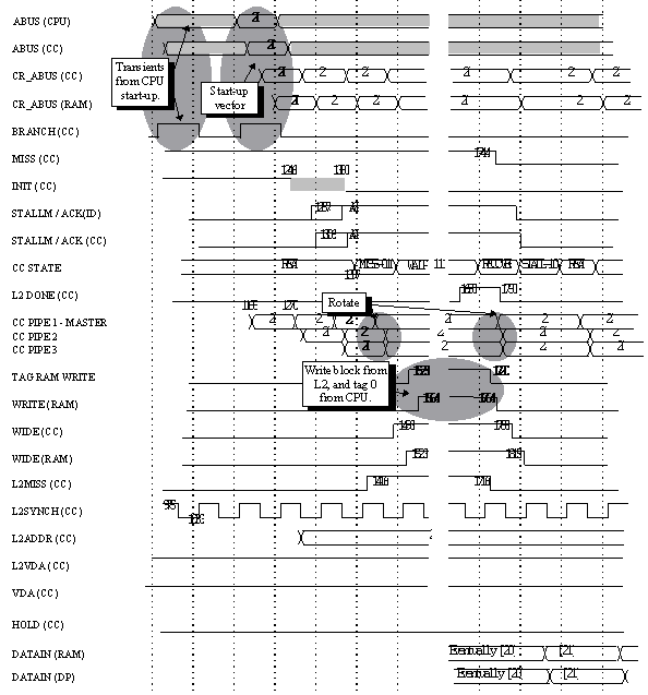
FIGURE 3.48: INSTRUCTION CACHE AT START-UP
The secondary cache will receive the global RESET
line (as well as all external trap and interrupt lines) and is
responsible for initializing the CPU and the cache in the proper
sequence.

Figure 3.49 illustrates the operation of the instruction cache during a page fault or during a trap which happens to occur coincidentally to a secondary cache transaction. The cache must take special measures to preserve the integrity of the tag RAM during such an event. When a page fault occurs, at least once primary cache (the one corresponding to the fault) is awaiting data from the secondary cache.
The primary cache will be in the WAIT state, with the tag RAM and cache RAM WRITE signals asserted. The cache RAMs will be performing a wide WRITE, awaiting the data from the secondary cache. The tag RAM will be writing in the new tag from the pipeline (originating from the CPU) along with the appropriate value of DIRTY. The old tag will have already been sent to the secondary cache during the READ stage of that memory access cycle.
When the trap occurs (presumably at the main memory level of the memory hierarchy in the case of a page fault), the trap is sent to the secondary cache. The secondary cache will then de-assert the L2VALID line. This bit is stored in the appropriate row of the tag RAM, along with the appropriate tag. If the bit is set to "valid," then future cache operations on that tag will proceed as normal. If, however, the data transfer from the secondary cache is interrupted by a trap, then the secondary cache sets the bit to "invalid," and if another operation takes place on that tag, it automatically causes a miss to take place.
In the event that a STORE into the data cache caused the page fault, it is questionable as to whether the transaction should be interrupted. If the cache were to simply mark the tag as invalid, the data stored by the CPU would be lost, and the CPU would have no way of knowing about it. Since STORE's are comparatively rare, and STORE misses even more so, the best decision is simply to stall the processor until the primary cache has valid data.
Since it takes approximately 500 ps to write into the tag RAM, and the data should be stable for a considerable period before that, the secondary cache should wait two cycles after de-asserting L2VALID before sending the trap signal through to the primary caches and CPU.
The primary cache responds to the trap signal by resetting to
the READ state. The MISS
signals may be spuriously asserted by the primary cache while
the trap is held high (the trap is tied to the INIT
signal pad), but the secondary cache has enough information to
ignore it, and the CPU ignores misses which occur while processing
the trap.
The design of the F-RISC / G prototype's primary cache imposes
certain constraints on the design of the secondary cache.

FIGURE 3.50: SECONDARY CACHE
BLOCK DIAGRAM
Figure 3.50 shows a block-diagram for a possible secondary cache configuration. A 32 kB Harvard architecture is assumed. Pipeline latches are included in order to enable the secondary cache to recover addresses in the event that a secondary cache miss occurs on an address that is eventually determined to be needed by the primary cache. (By the time the L2MISS signal issued by the primary cache reaches the secondary cache, the secondary cache may have received two additional addresses. If an additional valid address is received before the correct data for the previous address is fetched from either the secondary cache data RAM or the tertiary cache, and the data for the previous address is needed by the primary cache, then the address must be stored in the secondary cache as the primary cache will not re-send it - when the primary cache determines the data is needed, it sends the address of the data already present in the primary cache, instead.)
A pipeline latch is needed on the data RAM outputs in order to
handle primary cache copyback situations.

FIGURE 3.51: LOAD COPYBACK
IN F-RISC / G CACHE
Figure 3.51 illustrates the interaction of the F-RISC / G caches during a load copyback. The primary cache sends an address to the secondary cache before it is determined whether the primary cache needs the address. By the time the miss signal is sent to the secondary cache, assuming the secondary cache has not received additional valid addresses (the primary cache will assert the L2VDA signal when a valid address is on the bus), the secondary cache has already had at least a cycle to perform a read. The secondary cache must finish the read, and, using the copyback address and data which is sent to the secondary cache following the L2MISS signal, perform a write. While the write is being performed, the data read from the secondary cache must be latched. Once the data on the bi-directional bus is no longer needed, the secondary cache can assert L2DONE signal and put the data on the bus (the data should be on the bus for a phase before L2DONE is asserted.)
If the secondary cache is interrupted from reading its data memory by a new incoming valid address, then, when the secondary cache receives the miss signal, it must retrieve the address and restart its access. This is all necessary assuming the cache RAMs are single-ported, and is due to the fact that a new address may be received once a cycle, but the cache RAM access time is expected to be on the order of three or four cycles. Further complicating the situation is the fact that the miss doesn't arrive until two cycles after the associated address.
It is important to note that the five cycle mean access time
for the secondary cache was based on calculations for the stall
component of CPI. Therefore, the required five cycle limit implies
that, on average, accesses to the secondary cache result in a
stall of only five cycles. Since, in the event of a primary cache
hit, the data is required at the CPU at approximately the same
time the secondary cache receives the miss signal in the event
of a primary cache miss, the five cycles allotted to the secondary
cache begin approximately when the secondary cache receives the
L2MISS signal. This means
that, on average, a primary cache read miss has 7 ns to be completed.
(The data cache has an additional phase, while the instruction
cache fast bits have one phase fewer).