|
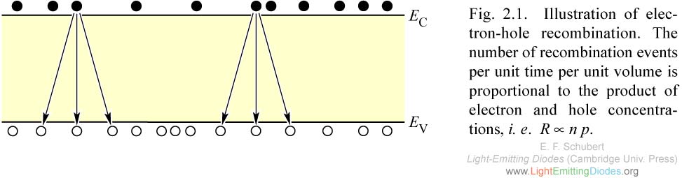
Fig. 2.1. Illustration of electron-hole recombination. The number of recombination events per unit time per unit volume is proportional to the product of electron and hole concentrations, i. e. R ∝ n p.
|
|
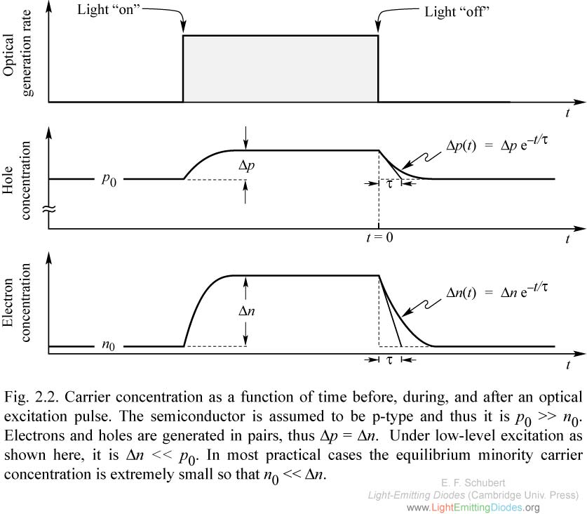
Fig. 2.2. Carrier concentration as a function of time before, during, and after an optical excitation pulse. The semiconductor is assumed to be p-type and thus it is p0 >> n0. Electrons and holes are generated in pairs, thus Delta p = Delta n. Under low-level excitation as shown here, it is Delta n << p0.
|
|
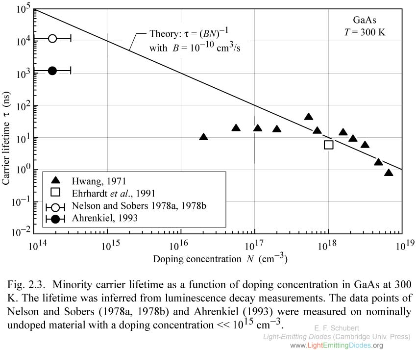
Fig. 2.3. Fig. 2.3. Minority carrier lifetime as a function of doping concentration in GaAs at 300 K. The lifetime was inferred from luminescence decay measurements. The data points of Nelson and Sobers (1978a, 1978b) and Ahrenkiel (1993) were measured on nominally undoped material with a doping concentration << 1015 cm-3.
|

|
Fig. 2.4. Fig. 2.4. (a) Luminescence decay for low and high excitation densities. (b) Time constants for low and high excitation densities. |
|
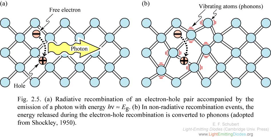
Fig. 2.5. Fig. 2.5. (a) Radiative recombination of an electronş-hole pair accompanied by the emission of a photon with energy hn ≈ Eg. (b) In non-radiative recombination events, the energy released during the electron-hole recombination is converted to phonons (adopted from Shockley, 1950).
|
|
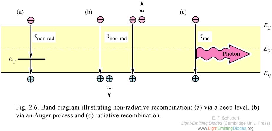
Fig. 2.6. Fig. 2.6. Band diagram illustrating non-radiative recombination: (a) via a deep level, (b) via an Auger process and (c) radiative recombination.
|

|
Fig. 2.7. Fig. 2.7. Cathodoluminescence micrograph of a GaAs epitaxial layer. The dark spots are due to large clusters of non-radiative recombination centers (after Schubert, 1995). |

|
Fig. 2.8. Fig. 2.8. Room-temperature photoluminescence spectrum of GaN with a band-to-band optical transition at 365 nm and a second transition at 550 nm identified as an optically active deep-level transition (after Grieshaber et al., 1996).
|
|
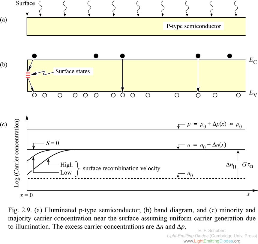
Fig. 2.9. Fig. 2.9. (a) Illuminated p-type semiconductor, (b) band diagram, and (c) minority and majority carrier concentration near the surface assuming uniform carrier generation due to illumination. The excess carrier concentrations are Delta n and Delta p.
|
|
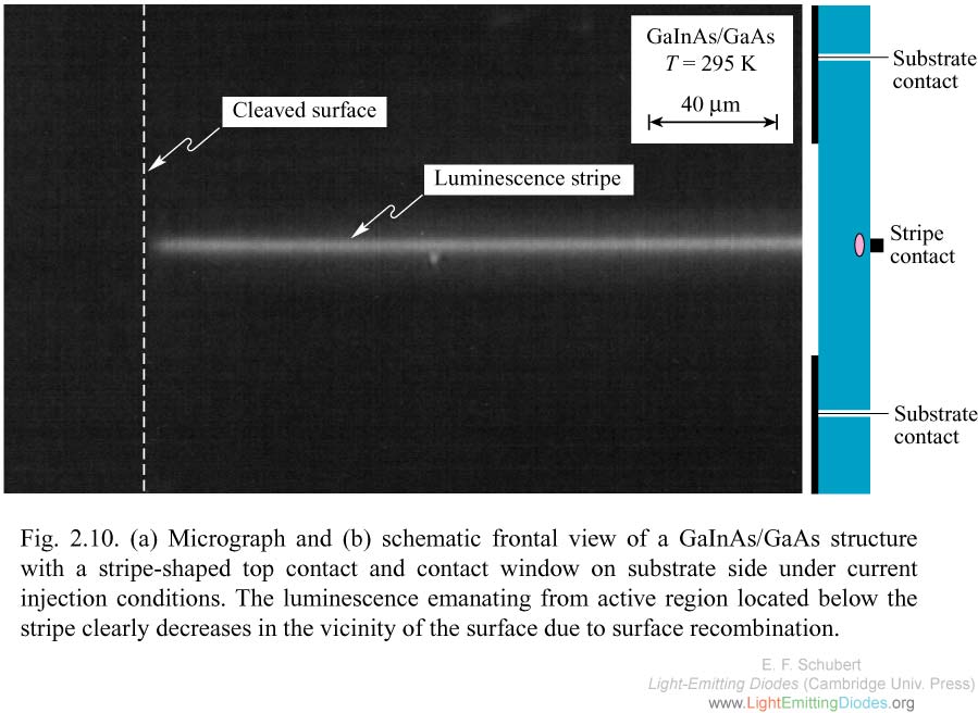
Fig. 2.10. Fig. 2.10. (a) Micrograph and (b) schematic frontal view of a GaInAs/GaAs structure with a stripe-shaped top contact and contact window on substrate side under current injection conditions.
|