|
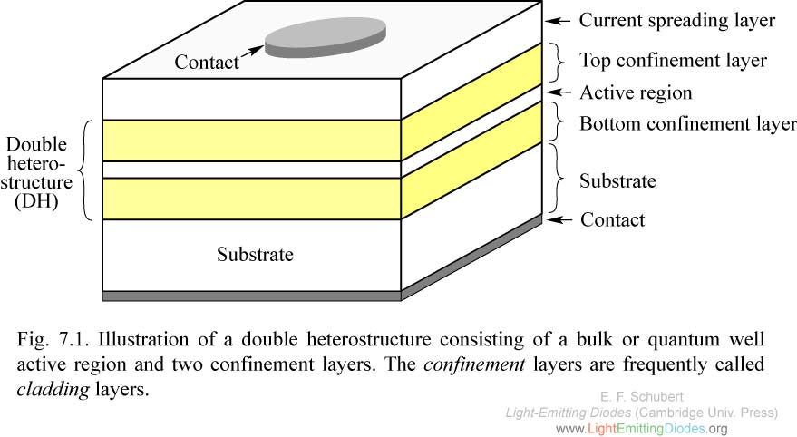
Fig. 7.1. Illustration of a double heterostructure consisting of a bulk or quantum well active region and two confinement layers. The confinement layers are frequently called cladding layers.
|
|
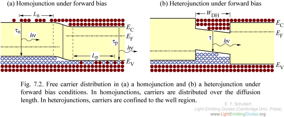
Fig. 7.2. Free carrier distribution in (a) a homojunction and (b) a heterojunction under forward bias conditions. In homojunctions, carriers are distributed over the diffusion length. In heterojunctions, carriers are confined to the well region.
|
|
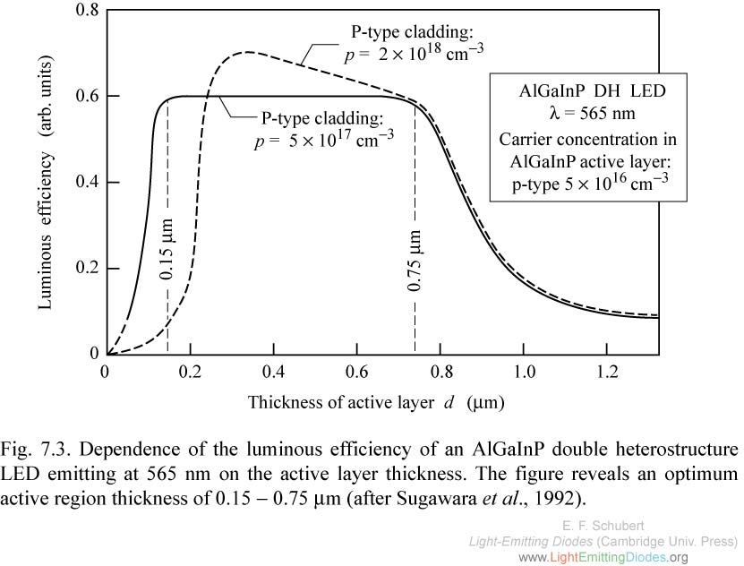
Fig. 7.3. Dependence of the luminous efficiency of an AlGaInP double heterostructure LED emitting at 565 nm on the active layer thickness. The figure reveals an optimum active region thickness of 0.15 - 0.75 mu m (after Sugawara et al., 1992).
|
|
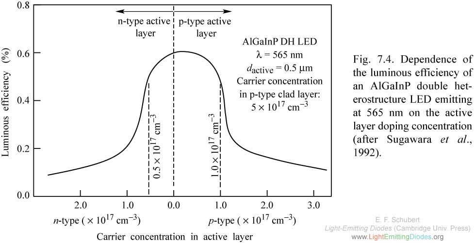
Fig. 7.4. Dependence of the luminous efficiency of an AlGaInP double heterostructure LED emitting at 565 nm on the active layer doping concentration (after Sugawara et al., 1992).
|
|
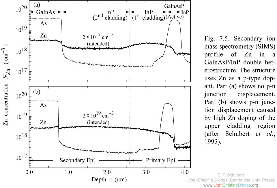
Fig. 7.5. Secondary ion mass spectrometry (SIMS) profile of Zn in a GaInAsP/InP double heterostructure. The structure uses Zn as a p-type dopant. Part (a) shows no p-n junction displacement. Part (b) shows p-n junction displacement caused by high Zn doping of the upper cladding region (after Schubert et al., 1995).
|
|
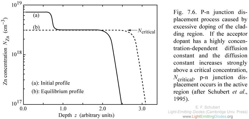
Fig. 7.6. P-n junction displacement process caused by excessive doping of the cladding region. |
|
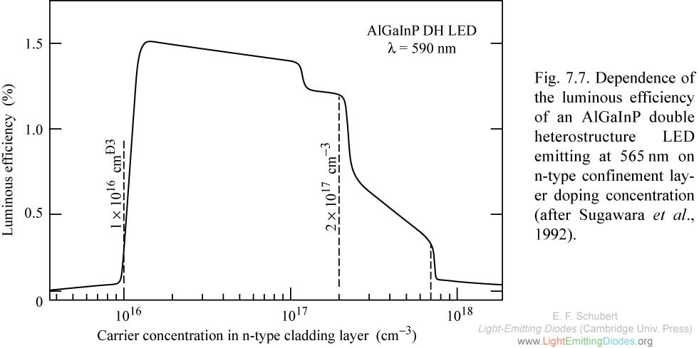
Fig. 7.7. Dependence of the luminous efficiency of an AlGaInP double heterostructure LED emitting at 565nm on n-type confinement layer doping concentration (after Sugawara et al., 1992).
|
|
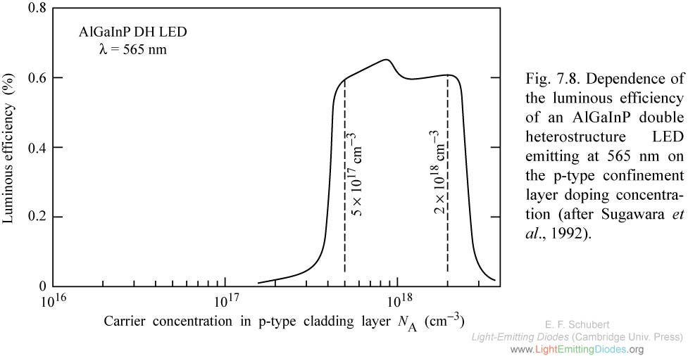
Fig. 7.8. Dependence of the luminous efficiency of an AlGaInP double heterostructure LED emitting at 565 nm on the p-type confinement layer doping concentration (after Sugawara et al., 1992).
|
|
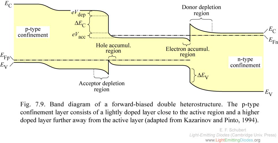
Fig. 7.9. Band diagram of a forward-biased double heterostructure. The p-type confinement layer consists of a lightly doped layer close to the active region and a higher doped layer further away from the active layer (adapted from Kazarinov and Pinto, 1994).
|
|
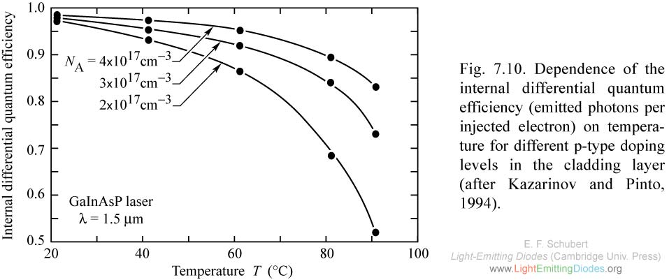
Fig. 7.10. Dependence of the internal differential quantum efficiency (emitted photons per injected electron) on temperature for different p-type doping levels in the cladding layer (after Kazarinov and Pinto, 1994).
|
|
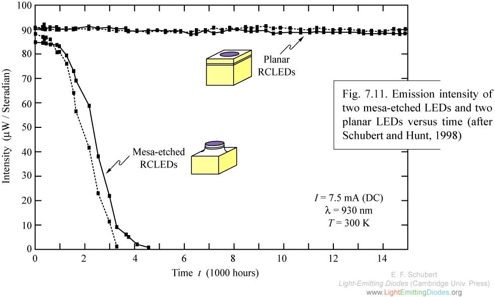
Fig. 7.11. Emission intensity of two mesa-etched LEDs and two planar LEDs versus time (after Schubert and Hunt, 1998).
|
|
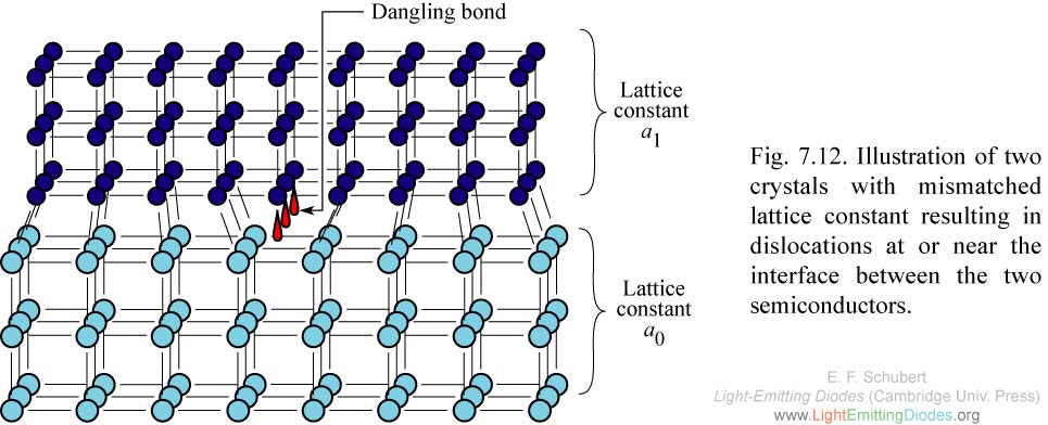
Fig. 7.12. Illustration of two crystals with mismatched lattice constant resulting in dislocations at or near the interface between the two semiconductors.
|
|
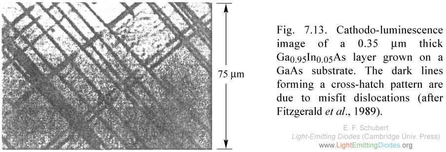
Fig. 7.13. Cathodo-luminescence image of a 0.35 mu m thick Ga0.95In0.05As layer grown on a GaAs substrate. The dark lines forming a cross-hatch pattern are due to misfit dislocations (after Fitzgerald et al., 1989).
|
|
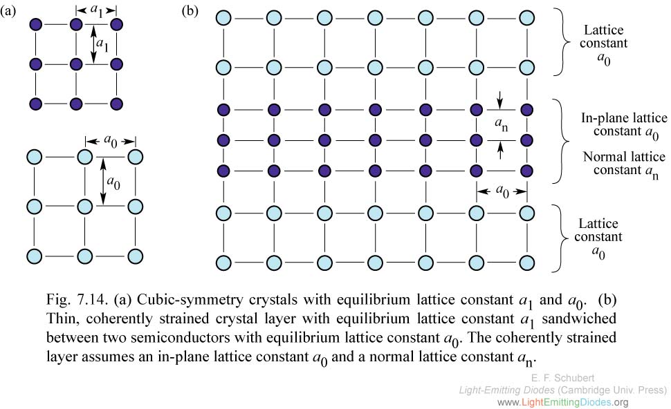
Fig. 7.14. (a) Cubic-symmetry crystals with equilibrium lattice constant a1 and a0. (b) Thin, coherently strained crystal layer with equilibrium lattice constant a1 sandwiched between two semiconductors with equilibrium lattice constant a0.
|
.jpg)
|
Fig. 7.15. Optical output in-tensity of an AlGaInP LED driven with an injection current of 20 mA versus the lattice mismatch between the AlInGaP active region and the GaAs substrate (after Watanabe and Usui, 1987).
|